Here we see the creeping sliding scale that is the terror of Age Verification. First of all, an OS does not need an age – it’s like saying any technology needs age verification: all gadgets use an OS, whether it is your washing machine, your smart light switch, your PSP or your PC. Second of all, an OS has no business being forced online – they are supposed to be non-cloud, personal, non-connected unless you want them to connect. Age verification requires external suppliers and so you would need to connect to perform the age verification – and send who knows what kind of other personal data. Eg Windows sends hardware data (along with a whole load of other data) that works much like a fingerprint. This makes it easy to track a users movements online. This is one reason why people want to bypass the online account creation on Windows and use local accounts.
As more US states consider online age-verification requirements, two Colorado lawmakers want to implement the age checks at the operating system-level, after California enacted a similar law.
Colorado’s SB26-051, introduced last month, would require operating systems to register the owner’s age, which third-party apps can then leverage to determine if the user is an adult. The bill calls for the device owner to register their birthdate or age, but for the purposes of creating an “age bracket,” which can then be shared to an app developer through an API to learn their age range, according to BiometricUpdate.com.
The bill comes from state Sen. Matt Ball and Rep. Amy Paschal, both Democrats. “The intent is to create thoughtful safeguards for kids online through a privacy-forward framework for age assurance,” Ball told PCMag. “Unlike some laws in other states, SB 51 doesn’t require users to share personally identifiable information or use facial recognition technology.”
Ball also said the legislation was based on California’s bill AB 1043, which was passed last year. It too requires OS makers to create a way for the device owner to register their age bracket, which can then be shared to app developers over an API. The California law starts to take effect January 1, 2027.
Ball added: “SB 26-51 is very closely modeled on it. One of the reasons for bringing SB 51 was that the tech and software industry is already complying with AB 1043, so there’s minimal added burden.”
Note here: they are not. Several Linux distributions have in fact already changed their ToU making it illegal for the software to be used in California.
The legislation also promises to centralize the age check through the OS, rather than mandating that each app enforce their own age-verification mechanism, which can involve scanning the user’s official ID, thus raising privacy and security concerns. The bill also forbids the sharing of the age-bracket data for any other purpose.
But it looks like it’s easy to bypass the age check proposed by SB26-051. The legislation itself doesn’t mention any state ID check to verify the owner’s age. In addition, the bill doesn’t seem to cover websites, only apps and app stores.
New research shows that behaviors that occur at the very lowest levels of the network stack make encryption—in any form, not just those that have been broken in the past—incapable of providing client isolation, an encryption-enabled protection promised by all router makers, that is intended to block direct communication between two or more connected clients.
The isolation can effectively be nullified through AirSnitch, the name the researchers gave to a series of attacks that capitalize on the newly discovered weaknesses. Various forms of AirSnitch work across a broad range of routers, including those from Netgear, D-Link, Ubiquiti, Cisco, and those running DD-WRT and OpenWrt.
AirSnitch “breaks worldwide Wi-Fi encryption, and it might have the potential to enable advanced cyberattacks,” Xin’an Zhou, the lead author of the research paper, said in an interview. “Advanced attacks can build on our primitives to [perform] cookie stealing, DNS and cache poisoning. Our research physically wiretaps the wire altogether so these sophisticated attacks will work. It’s really a threat to worldwide network security.” Zhou presented his research on Wednesday at the 2026 Network and Distributed System Security Symposium.
Paper co-author Mathy Vanhoef, said a few hours after this post went live that the attack may be better described as a Wi-Fi encryption “bypass,” “in the sense that we can bypass client isolation. We don’t break Wi-Fi authentication or encryption. Crypto is often bypassed instead of broken. And we bypass it ;)” People who don’t rely on client or network isolation, he added, are safe.
[…]
The lowest level, Layer-1, encompasses physical devices such as cabling, connected nodes, and all the things that allow them to communicate. The highest level, Layer-7, is where applications such as browsers, email clients, and other Internet software run. Levels 2 through 6 are known as the Data Link, Network, Transport, Session, and Presentation layers, respectively.
Identity crisis
Unlike previous Wi-Fi attacks, AirSnitch exploits core features in Layers 1 and 2 and the failure to bind and synchronize a client across these and higher layers, other nodes, and other network names such as SSIDs (Service Set Identifiers). This cross-layer identity desynchronization is the key driver of AirSnitch attacks.
The most powerful such attack is a full, bidirectional machine-in-the-middle (MitM) attack, meaning the attacker can view and modify data before it makes its way to the intended recipient. The attacker can be on the same SSID, a separate one, or even a separate network segment tied to the same AP. It works against small Wi-Fi networks in both homes and offices and large networks in enterprises.
[…]
Even when HTTPS is in place, an attacker can still intercept domain look-up traffic and use DNS cache poisoning to corrupt tables stored by the target’s operating system. The AirSnitch MitM also puts the attacker in the position to wage attacks against vulnerabilities that may not be patched. Attackers can also see the external IP addresses hosting webpages being visited and often correlate them with the precise URL.
Given the range of possibilities it affords, AirSnitch gives attackers capabilities that haven’t been possible with other Wi-Fi attacks, including KRACK from 2017 and 2019 and more recent Wi-Fi attacks that, like AirSnitch, inject data (known as frames) into remote GRE tunnels and bypass network access control lists.
“This work is impressive because unlike other frame injection methods, the attacker controls a bidirectional flow,” said HD Moore, a security expert and the founder and CEO of runZero.
[…]
The MitM targets Layers 1 and 2 and the interaction between them. It starts with port stealing, one of the earliest attack classes of Ethernet that’s adapted to work against Wi-Fi. An attacker carries it out by modifying the Layer-1 mapping that associates a network port with a victim’s MAC—a unique address that identifies each connected device. By connecting to the BSSID that bridges the AP to a radio frequency the target isn’t using (usually a 2.4GHz or 5GHz) and completing a Wi-Fi four-way handshake, the attacker replaces the target’s MAC with one of their own.
The attacker spoofs the victim’s MAC address on a different NIC, causing the internal switch to mistakenly associate the victim’s address with the attacker’s port/BSSID. As a result, frames intended for the victim are forwarded to the attacker and encrypted using the attacker’s PTK. Credit: Zhou et al.
In other words, the attacker connects to the Wi-Fi network using the target’s MAC and then receives the target’s traffic. With this, an attacker obtains all downlink traffic (data sent from the router) intended for the target. Once the switch at Layer-2 sees the response, it updates its MAC address table to preserve the new mapping for as long as the attacker needs.
This completes the first half of the MitM, allowing all data to flow to the attacker. That alone would result in little more than a denial of service for the target. To prevent the target from noticing—and more importantly, to gain the bidirectional MitM capability needed to perform more advanced attacks—the attacker needs a way to restore the original mapping (the one assigning the victim’s MAC to the Layer-1 port). An attacker performs this restoration by sending an ICMP ping from a random MAC. The ping, which must be wrapped in a Group Temporal key shared among all clients, triggers replies that cause the Layer-1 mapping (i.e., port states) to revert back to the original one.
“In a normal Layer-2 switch, the switch learns the MAC of the client by seeing it respond with its source address,” Moore explained. “This attack confuses the AP into thinking that the client reconnected elsewhere, allowing an attacker to redirect Layer-2 traffic. Unlike Ethernet switches, wireless APs can’t tie a physical port on the device to a single client; clients are mobile by design.”
The back-and-forth flipping of the MAC from the attacker to the target, and vice versa, can continue for as long as the attacker wants. With that, the bidirectional MitM has been achieved. Attackers can then perform a host of other attacks, both related to AirSnitch or ones such as the cache poisoning discussed earlier. Depending on the router the target is using, the attack can be performed even when the attacker and target are connected to separate SSIDs connected by the same AP. In some cases, Zhou said, the attacker can even be connected from the Internet.
“Even when the guest SSID has a different name and password, it may still share parts of the same internal network infrastructure as your main Wi-Fi,” the researcher explained. “In some setups, that shared infrastructure can allow unexpected connectivity between guest devices and trusted devices.”
Although port stealing was originally devised for hosts on the same switch, we show that attackers can hijack MAC-to-port mappings at a higher layer, i.e., at the level of the distribution switch—to intercept traffic to victims associated with different APs. This escalates the attack beyond its traditional limits, breaking the assumption that separate APs provide effective isolation.
This discovery exposes a blind spot in client isolation: even physically separated APs, broadcasting different SSIDs, offer ineffective isolation if connected to a common distribution system. By redirecting traffic at the distribution switch, attackers can intercept and manipulate victim traffic across AP boundaries, expanding the threat model for modern Wi-Fi networks.
[…]
AirSnitch, by contrast, requires that the attacker already have some sort of access to the Wi-Fi network. For many people, that may mean steering clear of public Wi-Fi networks altogether.
If the network is properly secured—meaning it’s protected by a strong password that’s known only to authorized users—AirSnitch may not be of much value to an attacker. The nuance here is that even if an attacker doesn’t have access to a specific SSID, they may still use AirSnitch if they have access to other SSIDs or BSSIDs that use the same AP or other connecting infrastructure.
[…]
“We expand the threat model showing an attacker can be on another channel or port, or can be from the Internet,” Zhou said. “Firewalls are also networking devices. We often say a firewall is a Layer-3 device because it works at the IP layer. But fundamentally, it’s connected by wire to different network elements. That wire is not secure.”
Some of the threat can be mitigated by using VPNs, but this remedy has all the usual drawbacks that come with them. For one, VPNs are notorious for leaking metadata, DNS queries, and other traffic that can be useful to attackers, making the protection limited.
[…]
Another potential mitigation is using wireless VLANs to isolate one SSID from another. Zhou said such options aren’t universally available and are also “super easy to be configured wrong.” Specifically, he said VLANs can often be implemented in ways that allow “hopping vulnerabilities.” Further, Moore has argued why “VLANs are not a practical barrier” against all AirSnitch attacks
The most effective remedy may be to adopt a security stance known as zero trust, which treats each node inside a network as a potential adversary until it provides proof it can be trusted. This model is challenging for even well-funded enterprise organizations to adopt, although it’s becoming easier. It’s not clear if it will ever be feasible for more casual Wi-Fi users in homes and smaller businesses.
Probably the most reasonable response is to exercise measured caution for all Wi-Fi networks managed by people you don’t know. When feasible, use a trustworthy VPN on public APs or, better yet, tether a connection from a cell phone.
[…]
“It will be interesting to see if the wireless vendors care enough to resolve these issues completely and if attackers care enough to put all of this together when there might be easier things to do (like run a fake AP instead),” Moore said. “At the least it should make pentesters’ lives more interesting since it re-opens a lot of exposure that many folks may not have any experience with.
This data breach should not have been so large. Yes, it’s good that Odido stood up to ransomware actors and did not pay the ransom. No, they should have deleted most of that data years and years ago as per their own TOS and EU regulation.
Odido is a Dutch telecommunications company and one of the largest mobile network operators in the Netherlands. It was formed when T-Mobile Netherlands and Tele2 were rebranded as Odido in 2023 after private equity firms Apax Partners and Warburg Pincus acquired the business.
Odido serves around 8 million mobile subscribers and about 1 million fixed broadband customers nationwide. The company provides mobile telephony, wireless broadband, and related services under multiple brands including Odido, Ben, and Simpel.
In mid-February, the cybercrime group ShinyHunters broke into the Dutch telecom firm Odido and accessed data from 6.2 million accounts. At the time, the company confirmed the breach and said attackers took names, addresses, phone numbers, email addresses, bank account details, dates of birth, and passport or ID numbers.
“Odido has been hit by a cyberattack, which compromised customer data. This involved personal data from a customer contact system used by Odido. No passwords, call logs, or billing information were affected.” reads a notice published by the company on its website. “The unauthorized access to the system was terminated as quickly as possible. Odido also engaged external cybersecurity experts to assist with implementing additional security measures as part of the incident response.”
The telco said the breach did not expose My Odido account passwords, call records, location data, invoice details, or scans of ID documents.
Odido’s subsidiary Ben also warned its customers that hackers may have stolen their information.
Now, an alleged final dump has exposed 4.6 million more unique email addresses from Dutch telecom provider Odido, bringing the total to 6.1 million across four separate releases.
“Due to recent developments regarding this telco, daily leaks will not happen anymore. Instead, you can download the Odido dataset concerning its full former and current customers below.” ShinyHunters wrote on its Tor data leak site. “Over 15m Salesforce records containing Full Names, Physical addresses, email addresses, phone numbers, and plaintext passwords, IBAN, passport numbers, driver license numbers and other internal corporate data have been compromised. This is your fault, Odido. You are the reason why an entire country is about to suffer for an unestimated amount of years. Unprecedented.”
The data breach notification service Have I Been Pwned (HIBP) added the compromised dataset to its archive. The final release includes a total of 6.1M unique addresses.
The Norwegian Consumer Council, a government funded organization advocating for consumer’s rights, released a report on the trend of “enshittification” in digital consumer goods and services, suggesting ways consumers for consumers to resist. But they’ve also dramatized the problem with a funny four-minute video about the man whose calls for him to make things shitty for people.
“It’s not just your imagination. Digital services are getting worse,” the video concludes — before adding that “Luckily, it doesn’t have to be this way.” The Consumer Council’s announcement recommends:
Stronger rights for consumers to control, adapt, repair, and alter their products and services,
Interoperability, data portability, and decentralisation as the norm, so the threshold for moving to different services becomes as low as possible,
Deterrent and vigorous enforcement of competition law, so that Big Tech companies are not allowed to indiscriminately acquire start-ups, competitors or otherwise steer the market to their advantage,
Better financing of initiatives to build, maintain or improve alternative digital services and infrastructure based on open source code and open protocols,
Reduce public sector dependence on big tech, to regain control and to contribute to a functioning market for service providers that respect fundamental rights,
Deterrent and consistent enforcement of other laws, including consumer and data protection law.
The Norwegian Consumer Council is also joining 58 organisations and experts in a letter asking the Norwegian government to rebalance power with enforcement resources and by prioritizing the procurement of services based on open source code. And “Our sister organisations are sending similar letters to their own governments in 12 countries.”
They’re also sending a second letter to the European Commission with 29 civil society organisations (including the EFF and Amnesty International) warning about the risks of deregulation and calling for reducing dependency on big tech.
So this is basically an agentic coordinator (which the correct technical term is an orchestrator). The agents are like microservices, or little programs designed to do a specific job – usually by interacting with a tool (eg a weather API). This is part of the puzzle that was missing in Agentic AI, but which an upstart coming from nowhere (OpenClaw) threw out there. Now we are seeing more of these coming out. It looks like people are copying OpenClaw pretty quickly.
The idea is that the user describes a specific outcome — something like “plan and execute a local digital marketing campaign for my restaurant” or “build me an Android app that helps me do a specific kind of research for my job.” Computer then ideates subtasks and assigns them to multiple agents as needed, running the models Perplexity deems best for those tasks. The core reasoning engine currently runs Anthropic’s Claude Opus 4.6, while Gemini is used for deep research, Nano Banana for image generation, Veo 3.1 for video production, Grok for lightweight tasks where speed is a consideration, and ChatGPT 5.2 for “long-context recall and wide search.”
This kind of best-model-for-the-task approach differs from some competing products like Claude Cowork, which only uses Anthropic’s models. All this happens in the cloud, with prebuilt integrations. “Every task runs in an isolated compute environment with access to a real filesystem, a real browser, and real tool integrations,” Perplexity says. The idea is partly that this workflow was what some power users were already doing, and this aims to make that possible for a wider range of people who don’t want to deal with all that setup.
People were already using multiple models and tailoring them to specific tasks based on perceived capabilities, while, for example, using MCP (Model Context Protocol) to give those models access to data and applications on their local machines. Perplexity Computer takes a different approach, but the goal is the same: have AI agents running tailor-picked models to perform tasks involving your own files, services, and applications. Then there is OpenClaw, which you could perceive as the immediate predecessor to this concept.
“The Diary of a Young Girl” is a Dutch language diary written by the young Jewish writer Anne Frank while she was in hiding for two years with her family during the Nazi occupation of the Netherlands. Although the diary and Anne Frank’s death in the Bergen-Belsen concentration camp are well known, few are aware that the text has a complicated copyright history – one that could have important implications for the legal status and use of Virtual Private Networks (VPNs) in the EU. TorrentFreak explains the copyright background:
These copyrights are controlled by the Swiss-based Anne Frank Fonds, which was the sole heir of Anne’s father, Otto Frank. The Fonds states that many print versions of the diary remain protected for decades, and even the manuscripts are not freely available everywhere.
In the Netherlands, for example, certain sections of the manuscripts remain protected by copyright until 2037, even though they have entered the public domain in neighboring countries like Belgium.
A separate foundation, the Netherlands-based Anne Frank Stichting, wanted to publish a scholarly edition of Anne Frank’s writing, at least in those parts of the world where her diary was in the public domain:
To navigate these conflicting laws, the Dutch Anne Frank Stichting published a scholarly edition online using “state-of-the-art” geo-blocking to prevent Dutch residents from accessing the site. Visitors from the Netherlands and other countries where the work is protected are met with a clear message, informing them about these access restrictions.
However, the Anne Frank Fonds was unhappy with this approach, and took legal action. Its argument was that such geo-blocking could be circumvented with VPNs, and so its copyrights in the Netherlands could be infringed upon by those using VPNs. The lower courts in the Netherlands dismissed this argument, and the case is now before the Dutch Supreme Court. Beyond the specifics of the Anne Frank scholarly edition, there are important issues regarding the use of VPNs to get around geo-blocking. Because of the potential knock-on effect the ruling in this case will have on EU law, the Dutch Supreme Court has asked for guidance from the EU’s top court, the Court of Justice of the European Union (CJEU).
The CJEU has yet to rule on the issues raised. But one of the court’s advisors, Advocate General Rantos, has published a preliminary opinion, as is normal in such cases. Although that advice is not binding on the CJEU, it often provides some indication as to how the court may eventually decide. On the main issue of whether the ability of people to circumvent geo-blocking is a problem, Rantos writes:
the fact that users manage to circumvent a geo-blocking measure put in place to restrict access to a protected work does not, in itself, mean that the entity that put the geo-blocking in place communicates that work to the public in a territory where access to it is supposed to be blocked. Such an interpretation would make it impossible to manage copyright on the internet on a territorial basis and would mean that any communication to the public on the internet would be global.
Moreover:
As the [European] Commission pointed out in its written observations, the holder of an exclusive right in a work does not have the right to authorise or prohibit, on the basis of the right granted to it in one Member State, communication to the public in another Member State in which that right has ceased to have effect.
Or, more succinctly: “service providers in the public domain country cannot be subject to unreasonable requirements”. That’s a good, common-sense view. But perhaps just as important is the following comment by Rantos regarding the use of VPNs to circumvent geo-blocking:
as the Commission points out in its observations, VPN services are legally accessible technical services which users may, however, use for unlawful purposes. The mere fact that those or similar services may be used for such purposes is not sufficient to establish that the service providers themselves communicate the protected work to the public. It would be different if those service providers actively encouraged the unlawful use of their services.
The hope has to be that the CJEU will agree with its Advocate General’s sensible and fair analysis, and will rule accordingly. But there is another important aspect to this story. The basic issue is that the Anne Frank Stichting wants to make its scholarly edition of Anne Frank’s diary available as widely as possible. That seems a laudable aim, since it will increase understanding and appreciation of the young woman’s remarkable diary by publishing an academically rigorous version. And yet the Anne Frank Fonds has taken legal action to stop that move, on the grounds that it would represent an infringement of its intellectual monopoly in some parts of Frank’s work, in some parts of the world. The current dispute is another clear example of how copyright has become for some an end in itself, more important than the things that it is supposed to promote.
The west is in the midst of the most serious assault on free speech and academic freedom since the heyday of McCarthyism seven decades ago. For years, we were told the danger came from the left: oversensitive students, censorious activists, no-platforming zealots. Yet the most aggressive and successful campaign to police speech in our public institutions is being waged by cheerleaders of a state currently committing genocide.
Consider a recent case. Last December, a pro-Israel lobby group, UK Lawyers for Israel (UKLFI), celebrated another apparent victory. It describes its mission as contributing “generally as lawyers to creating a supportive climate of opinion in the United Kingdom towards Israel”. In practice, this has meant lawfare, directed not only at pro-Palestinian activism, but at the public existence of Palestinian identity itself.
The offence this time? The Open University’s use of the term “ancient Palestine” to describe the birthplace of the Virgin Mary, which UKLFI argued was “historically inaccurate”. More than that, they argued it risked erasing “Jewish historical identity”, potentially breaching the Equality Act 2010 by creating “a hostile or offensive learning environment for Jewish and Israeli students”.
The OU’s Palestine Solidarity Group responded with a freedom of information request to see how their institution had handled the complaint. The reply from the OUwas clear. “Ancient Palestine” was “academically appropriate”. The fifth-century BC Greek historian Herodotus used the term Palestine to describe a region broader than that acknowledged by UKLFI. While the lobby group insisted Mary was born in the “predominantly Jewish region” of Galilee, the university noted that there is no academic consensus that Mary existed at all, still less where she was born.
That should have been the end of the matter. But instead, the OU conceded that “associations of this term with Roman colonial rule and with the contemporary political context require us to think about the meaning of the term to current and future students”. Academics did not “want the use of the term to imply or be read as a comment on the conflict between Israel and Palestine”, it added. In response to the UKLFI complaint, staff accepted that “the term is now problematic in a way that, perhaps, it was not when the materials were written in 2018”.
And so, despite affirming the term’s historical accuracy, the OU agreed to “not use the term ‘ancient Palestine’ in any future course materials”, and to “explain and contextualise its use in existing materials for current learners”. Last month, staff received an internal bulletin confirming the university had “agreed to change references to ‘Ancient Palestine’”, complete with a link to the UKLFI’s triumphant press release: “Open University agrees to change use of ‘ancient Palestine’ following UKLFI intervention.”
Strip away the bureaucratic phrasing and the picture is stark. A university accepted that a historically accurate term would be removed from future teaching because a partisan lobbying organisation objected to its claimed contemporary political resonance. “This is a despicable attempt by political hacks to dictate academic terminology,” says the esteemed historian Rashid Khalidi, author of The Hundred Years’ War on Palestine. “Every reputable history covering periods from ancient history to the present uses the term ‘Palestine,’ including scores of works by distinguished Israeli scholars.”
Enter the Higher Education (Freedom of Speech) Act 2023, introduced by the last Conservative government amid warnings that leftwing activists were strangling academic debate. The act imposes a duty on universities to secure lawful freedom of speech, even where that speech “may be offensive or hurtful to some”.
The OU had landed themselves in a mess. When the Palestine Solidarity Group argued that censoring an academically defensible term on the grounds that it was politically “problematic” violated the 2023 legislation, the vice-chancellor circulated a clarifying note: the university stood by academic freedom. The school would continue using the term, albeit with “an additional contextual note to support students’ understanding of differing perspectives”. His statement failed to say whether this change was a response to the intervention by a partisan lobby group.
[…]
This is just one example of UKLFI’s assault on Palestinian identity, past and present. Months before Israel’s genocide began, Chelsea and Westminster hospital removed a display of artwork by Palestinian children after a complaint by UKLFI claimed it made Jewish patients feel “vulnerable, harassed and victimised”. A pro-Palestinian concert planned at Morley College in London was cancelled after a UKLFI complaint in 2024. The group also sought to cancel the Falastin film festival in Scotland.skip past newsletter promotion
The Solicitors Regulation Authority is now investigating a complaint alleging that eight of UKLFI’s letters “demonstrate a seeming pattern of vexatious and legally baseless correspondence aimed at silencing and intimidating Palestine solidarity efforts”. Whatever the outcome of that investigation, the wider context is impossible to ignore.
[…]
This is the real crisis of free speech in the west. The target is not just protest, but a people. Israel seeks to erase Palestinians as a society. First they are destroyed in the present. Then they are deleted from the past.
The U.S. has used LUCAS kamikaze drones for the first time in combat, U.S. Central Command acknowledged on Saturday. The drones, based on the Iranian Shahed-136, were launched from the ground by Task Force Scorpion Strike (TFSS). The task force was set up in December “to flip the script on Iran,” a U.S. official told us at the time. The launch of LUCAS drones marks a rare instance when the U.S. adopted Iran’s drone playbook and used it against them.
Today’s strikes were part of Operation Epic Fury, an attack the U.S. launched along with Israel on targets across Iran. You can read more about that in our initial story here.
The LUCAS drones are designed to be a far less expensive strike weapon than missiles, which not only cost more, but are far more difficult and time-consuming to produce.
“Costing approximately $35,000 per platform, LUCAS is a low-cost, scalable system that provides cutting-edge capabilities at a fraction of the cost of traditional long-range U.S. systems that can deliver similar effects,” Navy Capt. Tim Hawkins, a CENTCOM spokesperson, told TWZ back in December. “The drone system has an extensive range and the ability to operate beyond line of sight, providing significant capability across CENTCOM’s vast operating area.”
In addition, the LUCAS design includes features that allow for “autonomous coordination, making them suitable for swarm tactics and network-centric strikes,” a U.S. official told us. As we have explained in detail in the past, the swarming capabilities combined with some of the drones being equipped with Starlink terminals, means extremely advanced cooperative tactics and dynamic targeting are possible, all while keeping humans in the loop.
The LUCAS drones have “an extensive range and are designed to operate autonomously,” CENTCOM said in a press release announcing the creation of Task Force Scorpion Strike. “They can be launched with different mechanisms to include catapults, rocket-assisted takeoff, and mobile ground and vehicle systems.”
Low-cost Unmanned Combat Attack System (LUCAS) drones are positioned on the tarmac at a base in the U.S. Central Command operating area, Nov. 23. Costing approximately $35,000 per platform, LUCAS drones are providing U.S. forces in the Middle East low-cost, scalable capabilities to strengthen regional security and deterrence. (Courtesy Photo)
Though the LUCAS drones fired against Iran were ground-launched, U.S. Navy personnel in the Middle East test-fired one from the Independence class Littoral Combat Ship (LCS) USS Santa Barbara. This came two weeks after the U.S. military announced the formation of Task Force Scorpion Strike.
Images that are generated with Stable Diffusion with QR Codes as ControlNet’s input, making the QR Code data points blend into the artwork while still being scannable by QR Code readers.
There are a few online services you can try, but this guide will focus on doing it locally on our own. You will need the basic knowledge of Stable Diffusion and ControlNet, a computer with a GPU (or a cloud GPU instance) to start.
GrapheneOS is a possible alternative to Android, but more open, more secure, more private. Since Google intends to lock down Android by releasing the code once per quarter and not allowing the installation of external apps without developers registering with Google (and paying for this), we need a secure, open OS alternative. With manufacturers partnering with GrapheneOS this is more likely to become a possibility.
Motorola, a Lenovo Company, announced the addition of new consumer and enterprise solutions to its portfolio today at Mobile World Congress. The company unveiled a partnership with the GrapheneOS Foundation, to bring cutting-edge security to everyday users across the globe. In addition, Motorola introduced a new Moto Secure feature and Moto Analytics, to expand Motorola’s B2B ecosystem with advanced security and deeper operational insights for organizations across industries. These announcements reinforce Motorola’s commitment to delivering intelligent, and highly capable technology with enhanced security for customers worldwide.
GrapheneOS Foundation Partnership Motorola is introducing a new era of smartphone security through a long‑term partnership with the GrapheneOS Foundation, the leading nonprofit in advanced mobile security and creators of a hardened, operating system based on the Android Open Source Project. Together, Motorola and the GrapheneOS Foundation will work to strengthen smartphone security and collaborate on future devices engineered with GrapheneOS compatibility.
Here we see the creeping sliding scale that is the terror of Age Verification. First of all, an OS does not need an age – it’s like saying any technology needs age verification: all gadgets use an OS, whether it is your washing machine, your smart light switch, your PSP or your PC. Second of all, an OS has no business being forced online – they are supposed to be non-cloud, personal, non-connected unless you want them to connect. Age verification requires external suppliers and so you would need to connect to perform the age verification – and send who knows what kind of other personal data. Eg Windows sends hardware data (along with a whole load of other data) that works much like a fingerprint. This makes it easy to track a users movements online. This is one reason why people want to bypass the online account creation on Windows and use local accounts.
For more on the horrors of age verification, see https://www.linkielist.com/?s=age+verification&submit=Search
The government of California is implementing a law that requires operating system providers to implement some form of age verification into their account setup procedures.
Assembly Bill No. 1043 was approved by California governor Gavin Newsom in October of last year, and becomes active on January 1, 2027 (via The Lunduke Journal). The bill states, among other factors, that “An operating system provider shall do all of the following:”
“(1) Provide an accessible interface at account setup that requires an account holder to indicate the birth date, age, or both, of the user of that device for the purpose of providing a signal regarding the user’s age bracket to applications available in a covered application store. Related articles
“(2) Provide a developer who has requested a signal with respect to a particular user with a digital signal via a reasonably consistent real-time application programming interface that identifies, at a minimum, which of the following categories pertains to the user.”
The categories are broken into four sections: users under 13 years of age, over 13 years of age under 16, at least 16 years of age and under 18, and “at least 18 years of age.”
In essence, while the bill doesn’t seem to require the most egregious forms of age verification (face scans or similar), it does require OS providers to collect age verification of some form at the account/user creation stage—and to be able to pass a segmented version of that information to outside developers upon request.
That’s likely no big deal for Windows, which already requires you to enter your date of birth during the Microsoft Account setup procedure. However, the idea that all operating system providers need to comply (in California) has drawn a fair degree of ire from certain Linux communities.
Keep up to date with the most important stories and the best deals, as picked by the PC Gamer team.Contact me with news and offers from other Future brandsReceive email from us on behalf of our trusted partners or sponsorsBy submitting your information you agree to the Terms & Conditions and Privacy Policy and are aged 16 or over.
“This is basically impossible for California to enforce” says CatoDomine on the Linuxmint subreddit. “Even if Linux Mint decides to add some kind of age verification, to comply with CA law, there’s no reason anyone would choose that version.”
2000 m above ground level (AGL), winds are stronger and much, much more consistent than they are at surface. Even if the Earth were a perfect sphere, there’d be a sluggish boundry layer at the surface, but since it’s got all these interesting bumps and bits and bobs, it’s not just sluggish but horribly turbulent, too. Getting above that, as much as possible, is why wind turbines are on big towers. Rather than build really big tower, Beijing Lanyi Yunchuan Energy Technology Co. has gone for a more ambitious approach: an aerostat to take power from the steady winds found at high altitude. Ambitiously called the Stratosphere Airborne Wind Energy System (SAWES), the megawatt-scale prototype has recently begun feeding into the grid in Yibin, Sichuan Province.
The name might be a bit ambitious, since its 2000 m test flight is only one tenth of the way to the stratosphere, but Yibin isn’t a bad choice for testing: as it is well inland, the S2000 prototype won’t have to contend with typhoons or other ocean storms. The prototype is arguably as ambitious as the name: its 12 flying turbines have a peak capacity of three megawatts. True, there are larger turbines in wind farms right now, but at 60 m in length and 40 m in diameter, the S2000 has a lot of room to grow before hitting any kind of limit or even record for aerostats. We’re particularly interested in the double-hull construction– it would seem the ring of the outer gas bag would do a good job funneling and accelerating air into those turbines, but we’d love to see some wind tunnel testing or even CFD renderings of what’s going on in there.
A rear view shows the 12 turbines inside the double hull. It should guide air into the gap, but we wonder how much turbulence the trusses in there are making.
During its first test flight in January 2026, the system generated generated 385 kilowatt-hours of electricity over the course of 30 minutes. That means it averaged about 25% capacity for the test, which is a good safe start. Doubtless the engineers have a full suite of test flights planned to demonstrate the endurance and power production capabilities of this prototype. Longer flights at higher capacity may have already happened by the time you read this.
Flying wind turbines isn’t a new idea by any means; a few years ago we featured this homemade kite generator, and the pros have been in on it too. Using helium instead represents an interesting design choice–on the plus side, its probably easier to control, and obviously allowing large structures, but the downside is the added cost of the gas. It will be interesting to see how it develops.
Azure Local can now run fully disconnected with no cloud connectivity, Microsoft confirmed at the London leg of its AI tour.
The latest change comes amid heightened trade and geopolitical tensions between the US administration and Europe, with more customers in the trading bloc seeking reassurances about digital sovereignty.
Like rival US hyperscalers, Microsoft has rolled out initiatives in Europe in a bid to address jittery locals worried about the possibility – no matter how remote – of service interruption or their data being accessed by American officials under the US CLOUD Act.
In March, Microsoft completed its EU Data Boundary service, then added more features in November. Yet for a growing number of organizations in Europe, only infrastructure under their direct control will do.
Azure Local (formerly Azure Stack HCI) is Microsoft’s answer to those concerns. Using specialized hardware, Azure Local lets customers run workloads on-premises. However, it still needed to phone home occasionally – its management via Azure Arc ran in the cloud, and pulling the plug for more than 30 days resulted in reduced functionality.
By making disconnected operations available in Azure Local, organizations can “now run mission-critical infrastructure with Azure governance and policy control, with no cloud connectivity, optimizing continuity for sovereign, classified or isolated environments,” Microsoft said this week.
In other words, no more calling back to the mothership.
Microsoft has also made Microsoft 365 Local available (think Exchange Server, SharePoint Server, and Skype for Business Server) and announced Foundry Local (only available to “qualified customers”).
“This brings the richness of Microsoft’s enterprise AI capabilities to on-premises systems, complete with local inferencing and APIs that operate completely within customer-controlled data boundaries,” Microsoft said.
Microsoft’s sovereignty claims may ring hollow for some after it admitted in France last year that it could not guarantee sovereignty if it were compelled to hand data to the US government. The ability to completely pull the plug is therefore intended to reassure customers, even if the software remains proprietary and supplied by a US tech giant.
[…]
“Sovereignty is increasingly a requirement, and we welcome any new services, tools, and software that can run in European Cloud Infrastructure Services Providers’ datacenters and on their own platforms. We look forward to testing these products against our forthcoming CISPE Sovereign Cloud Services Framework to see if they qualify for a Sovereign Badge or a Resilient Badge.”
[…]
Microsoft is not the only tech giant concerned about sovereignty. Amazon Web Services made its European Sovereign Cloud generally available earlier this year, and Google is selling customers a variety of solutions, including Google Cloud Airgapped, which runs on servers fully disconnected from the internet.
Whether these efforts satisfy customers will hinge on implementation and on how sovereignty is defined. Being able to disconnect completely will satisfy some, though others may still worry that the software remains under Microsoft’s control.
An editor who works for YouTube’s biggest creator, MrBeast, has been suspended from the prediction market platform Kalshi and reported to federal regulators for insider trading, Kalshi officials said on Wednesday. It’s the first time the company has publicly revealed the results of an investigation into market manipulation on the popular app.
The MrBeast employee, who Kalshi identified as Artem Kaptur in regulatory filings, traded around $4,000 on markets related to the streamer, the company said.
But Kalshi investigators say Kaptur was using proximity to the streamer as a way of trying to make quick cash. Using confidential information to manipulate markets is prohibited by Kalshi’s rules and could violate federal law.
“We investigated and found that the trader was employed as an editor for the streamer’s show and likely had access to material non-public information connected to his trading,” said Robert DeNault, the company’s head of enforcement.
Kalshi said the company froze the account in question, so Kaptur was not able to withdraw any profits. He was fined $20,000 and suspended from the platform for two years. Kalshi also said the case was reported to regulators at the Commodity Futures Trading Commission, or CFTC, which oversees prediction markets like Kalshi.
[…]
Another trading case involved a former political candidate
Kalshi also unveiled a case against a former longshot Republican candidate in the California governor’s race, Kyle Langford, who posted on X in May that he bet on himself to win the statewide contest. He encouraged others to do the same.
While it appeared to be a social media stunt, it was also a violation of Kalshi’s rules, and regulators said potentially a federal crime.
In a legal notice made public Wednesday, officials at Kalshi said that as a candidate, Langford was “a direct decision maker” for the market on the state’s governor’s race, prohibiting him from betting under internal guidelines against insider trading and market manipulation.
Kalshi banned Langford for five years from its platform and handed him a $2,200 fine.
“As a candidate in a race, you can (and probably should) follow and use Kalshi’s market forecast, but you should not trade on it,” Kalshi’s DeNault said.
[…]
Online prediction market platforms, such as Polymarket and Kalshi, have seen a surge in popularity during Trump’s second term. People can place bets on these platforms on wide-ranging issues such as what words people say at events, the outcome of elections or how much snow will fall in New York City.
The explosive growth of the industry is in part driven by the use of what observers many consider a legal loophole, which the Trump administration supports.
Instead of falling under the purview of state gambling laws, prediction markets are regulated in a more obscure way, as a type of “futures contract,” overseen by CFTC, which typically regulates bets on the future production of things like soybeans, corn and crude oil.
The Biden administration fought prediction market apps from listing most types of contracts. It argued there was little public interest value in most of them, not to mention that they invite speculators to manipulate markets through insider trading.
[…]
Until recently, regulators had allowed a few dozen markets a year for futures trading. Now, there are more than 200,000 active prediction markets.
The burgeoning and controversial industry has run headlong into global affairs. In January, a trader made $400,000 in profit on Polymarket by placing a successful bet on the capture of the Venezuelan leader Nicolás Maduro before there was any public indication that would happen.
Earlier this month, Israeli authorities arrested several people and charged two on suspicion of using classified information to place bets about upcoming military operations in Iran on Polymarket.
Insider trading on Polymarket and Kalshi is prohibited by each platform’s rules, and is illegal under federal law, but experts say each company’s internal systems can only catch so much insider activity, which can take place by word of mouth or other means outside the prediction market apps.
Still, Kalshi says in the past year it has opened 200 investigations into insider trading, 12 of which are still ongoing.
Months later, in November, crypto exchange giant FTX halted withdrawals and filed for bankruptcy. Customer funds had allegedly been diverted without consent to cover losses at sister trading firm Alameda Research, fund real estate, political donations, and other unapproved uses. The amount of money that was diverted is somewhat disputed, but what’s clear is that customers were unable to receive requested crypto withdrawals. Bitcoin bottomed below $20,000 amid the broader deleveraging, and reports later pointed to ties between the two crypto disasters.
Justice delivered partial accountability. Do Kwon, Terraform Labs co-founder, pleaded guilty to fraud and manipulation charges tied to misleading investors about UST’s stability. He received a 15-year prison sentence this past December, with victims testifying to the widespread destruction. Sam Bankman-Fried was convicted on seven counts, including wire fraud, securities fraud, and money laundering for the FTX misconduct. A judge sentenced him to 25 years in March 2024 and ordered $11 billion in forfeiture.
Both Bankman-Fried and lawyers associated with Terraform Labs are now working to recast their respective roles in the collapses.
Was FTX Actually Insolvent?
From prison, Bankman-Fried has posted on X claiming FTX was never technically insolvent. In a recent “10 Myths About Me & FTX” thread, he states the platform held more assets than liabilities, could have repaid customers in kind, and is now delivering 119-143% recoveries. He blames bankruptcy professionals for rushing a Chapter 11 filing, charging over $1 billion in fees, and dismantling the estate instead of allowing an orderly wind-down.
Most crypto industry insiders, where Bankman-Fried is viewed as the ultimate villain, dismiss this general argument. If assets were truly sufficient, withdrawals would not have been frozen. New York University Stern School of Business Adjunct Professor Austin Campbell noted that solvency for a crypto exchange means holding customer assets in the exact form and availability they expect, adding, “FTX did not have that. They were insolvent.” Galaxy Head of Firmwide Research Alex Thorn added that diverting deposits into illiquid bets against customers’ wishes amounts to theft, making the platform insolvent the moment redemptions failed.
Bankman-Fried has also used his public posts to court a pardon from President Trump. The White House told Fortune this week that no pardon is in the works or planned.
Terraform Labs Blames Insider Traders Instead of Their Broken Stablecoin Model
Let’s be extremely clear. UST failed because it was a ponzi scheme. It was a criminal enterprise that lured depositors with promise of high yield, paid from the deposits of new entrants. There is no possible universe where it didn’t go broke.
According to the new complaint, Jane Street allegedly obtained non-public information from Terraform insiders through private communication channels established by its employee and former Terraform member Bryce Pratt, who maintained contact with former colleagues, including a software engineer and the head of business development. A specific allegation involves May 7, 2022, when Terraform Labs withdrew 150 million UST from the Curve3pool without any public announcement; within 10 minutes, a wallet linked to Jane Street withdrew an additional 85 million UST from the same pool.
The bacteria that live inside our digestive tract undoubtedly play a vital part in our health. But buyer beware of companies that claim to have deciphered the gut microbiome. Research out today shows that no two at-home tests will tell you the same thing.
Government scientists sent standardized fecal samples to seven different gut health testing companies. The companies returned results that varied from one another, sometimes dramatically, while one company’s tests couldn’t conclusively decide if the same samples belonged to a healthy microbiome or not. The findings indicate that customers shouldn’t put too much stock in these tests, at least right now, the researchers say.
“Our results demonstrate the need for standards to ensure analytical validity and consumer confidence,” the authors wrote in their paper, published Thursday in Communications Biology.
Not quite there yet
Exciting as the field of gut health is, it’s very much in its infancy. We’re still not quite sure exactly what makes for a healthy mix of bacteria in our guts, much less how to reliably fix an unhealthy microbiome (it’s likely there are many different combinations of bacteria that could be “healthy”). And we’re still trying to untangle the complex interactions between our gut bacteria and various health conditions.
This uncertainty hasn’t stopped several companies from entering the direct-to-consumer industry, however. While some may be cautious in their advertising, others have claimed their tests can tell whether a person’s microbiome is healthy, and they might even sell products that will supposedly restore a dysfunctional one. Many scientists have already called for tighter regulation of these tests. Researchers at the National Institute of Standards and Technology, a division of the U.S. Department of Commerce, and others sought to gauge the reliability of these tests across different companies.
Open source projects, ever short of funding, have a potential new source of revenue in the form of the Open Source Endowment (OSE).
The organization describes itself as “the world’s first endowment fund for open source software.”
There are certainly other organizations that help fund open source software, such as Open Collective, Open Source Collective, and the Rust Foundation’s Maintainers Fund, not to mention organizations like the Software Freedom Conservancy, which provides legal and infrastructure support to open source projects. Open source developers may also be fortunate enough to receive contributions from individuals, companies (when not passing the buck), and government-sponsored initiatives like Germany’s Sovereign Tech Fund.
But OSE aspires specifically to build a big pile of cash – an endowment – that it will dole out to deserving open source projects.
It’s certainly needed. In 2023, Denis Pushkarev, maintainer of the widely used core-js library, vented his frustration with the fact that users of his software seldom offer financial support. “Free open source software is fundamentally broken,” he said.
The year before that, Christofer Dutz – creator of Apache PLC4X – lamented uncompensated use of his software. Earlier in 2022, Google talked up the need to support critical open source infrastructure, citing the log4j vulnerability.
But concerns about the sustainability of open source go back further still. Two years after the 2014 Heartbleed vulnerability – a dangerous flaw in OpenSSL – a Ford Foundation report noted that the OpenSSL project is critical internet infrastructure yet had just one full-time maintainer and earned less than $2,000 per year in donations.
As OSE points out, 95 percent of codebases rely on open source software, each of which has an average of 500 open source components. And yet 86 percent of open source contributors receive no payment for their work.
OSE founding chairman Konstantin Vinogradov, a venture capital investor, previously said he wanted to replicate the funding model that has sustained universities.
And he reiterated that aspiration in a Hacker News post announcing OSE.
Universities and the open source community, he argues, share reputation-based culture and functions, working together to create valuable ideas for the benefit of the public, educating each other, and commercializing only a portion of what’s produced.
“For universities, humanity has just two sustainable funding models: public spending or private endowments,” Vinogradov explained. “Government support won’t work for OSS at scale – it’s too globally decentralized. And yet nobody had built an OSS-focused endowment before. After understanding why, I started building one together with other OSS folks.”
Vinogradov said the OSE, a US 501(c)(3) tax-exempt charity, aims to make open source development more sustainable through a community-driven endowment. Donations will be invested and only investment income will be disbursed through grants – the principal funds will remain invested in the hope of growth.
Presently, the fund stands at around $700,000, thanks to contributions from more than 60 founding donors, including the founders of ClickHouse, curl, Elastic, Gatsby, HashiCorp, n8n, Nginx, Pydantic, Supabase, and Vue.js.
Donations go directly to the fund, and those who give over $1,000 can become OSE Members, which includes certain rights to participate in OSE governance.
According to Vinogradov, “OSE won’t give money for commercial product development – it is dedicated to supporting existing highly-used nonprofit and independent OSS.”
As many of the AI stories on Walled Culture attest, one of the most contentious areas in the latest stage of AI development concerns the sourcing of training data. To create high-quality large language models (LLMs) massive quantities of training data are required. In the current genAI stampede, many companies are simply scraping everything they can off the Internet. Quite how that will work out in legal terms is not yet clear. Although a few court cases involving the use of copyright material for training have been decided, many have not, and the detailed contours of the legal landscape remain uncertain.
However, there is an alternative to this “grab it all” approach. It involves using materials that are either in the public domain or released under a “permissive” licence that allows LLMs to be trained on them without any problems. There’s plenty of such material online, but its scattered nature puts it at a serious disadvantage compared to downloading everything without worrying about licensing issues. To address that, the Common Corpus was created and released just over a year ago by the French startup Pleias. A press release from the AI Alliance explains the key characteristics of the Common Corpus:
Truly Open: contains only data that is permissively licensed and provenance is documented
Multilingual: mostly representing English and French data, but contains at least 1[billion] tokens for over 30 languages
Diverse: consisting of scientific articles, government and legal documents, code, and cultural heritage data, including books and newspapers
Extensively Curated: spelling and formatting has been corrected from digitized texts, harmful and toxic content has been removed, and content with low educational content has also been removed.
There are five main categories of material: OpenGovernment, OpenCulture, OpenScience, OpenWeb, and OpenSource:
OpenGovernment contains Finance Commons, a dataset of financial documents from a range of governmental and regulatory bodies. Finance Commons is a multimodal dataset, including both text and PDF corpora. OpenGovernment also contains Legal Commons, a dataset of legal and administrative texts. OpenCulture contains cultural heritage data like books and newspapers. Many of these texts come from the 18th and 19th centuries, or even earlier.
OpenScience data primarily comes from publicly available academic and scientific publications, which are most often released as PDFs. OpenWeb contains datasets from YouTube Commons, a dataset of transcripts from public domain YouTube videos, and websites like Stack Exchange. Finally, OpenSource comprises code collected from GitHub repositories which were permissibly licensed.
The initial release contained over 2 trillion tokens – the usual way of measuring the volume of training material, where tokens can be whole words and parts of words. A significant recent update of the corpus has taken that to over 2.267 trillion tokens. Just as important as the greater size, is the wider reach: there are major additions of material from China, Japan, Korea, Brazil, India, Africa and South-East Asia. Specifically, the latest release contains data for eight languages with more than 10 billion tokens (English, French, German, Spanish, Italian, Polish, Greek, Latin) and 33 languages with more than 1 billion tokens. Because of the way the dataset has been selected and curated, it is possible to train LLMs on fully open data, which leads to auditable models. Moreover, as the original press release explains:
By providing clear provenance and using permissibly licensed data, Common Corpus exceeds the requirements of even the strictest regulations on AI training data, such as the EU AI Act. Pleias has also taken extensive steps to ensure GDPR compliance, by developing custom procedures to enable personally identifiable information (PII) removal for multilingual data. This makes Common Corpus an ideal foundation for secure, enterprise-grade models. Models trained on Common Corpus will be resilient to an increasingly regulated industry.
Another advantage for many users is that material with high “toxicity scores” has already been removed, thus ensuring that any LLMs trained on the Common Corpus will have fewer problems in this regard.
The Common Corpus is a great demonstration of the power of openness and permissive copyright licensing, and how they bring benefits that other approaches can’t match. For example: “Common Corpus makes it possible to train models compatible with the Open Source Initiative’s definition of open-source AI, which includes openness of use, meaning use is permitted for ‘any purpose and without having to ask for permission’. ” That fact, along with the multilingual nature of the Common Corpus, would make the latest version a great fit for any EU move to create “public AI” systems, something advocated on this blog a few months back. The French government is already backing the project, as are other organisations supporting openness:
The Corpus was built up with the support and concerted efforts of the AI Alliance, the French Ministry of Culture as part of the prefiguration of the service offering of the Alliance for Language technologies EDIC (ALT-EDIC).
This dataset was also made in partnership with Wikimedia Enterprise and Wikidata/Wikimedia Germany. We’re also thankful to our partner Libraries Without Borders for continuous assistance on extending low resource language support.
The corpus was stored and processed with the generous support of the AI Alliance, Jean Zay (Eviden, Idris), Tracto AI, Mozilla.
The unique advantages of the Common Corpus mean that more governments should be supporting it as an alternative to proprietary systems, which generally remain black boxes in terms of where their training data comes from. Publishers too would also be wise to fund it, since it offers a powerful resource explicitly designed to avoid some of the thorniest copyright issues plaguing the generative AI field today.
In quantum mechanics, the idea that quantum information can’t be duplicated is ironclad – or at least, it was. A surprising approach to backing up qubits, the basic units of quantum computers, appears to allow a sidestepping of this fundamental law of physics.
The no-cloning theorem was first discovered by researchers in the 1980s. It says that quantum states that describe all the information about a system can’t be copied. Attempting to measure the information to copy it would simply destroy the delicate quantum properties that you want to measure. This fact has proved important for quantum technologies like encryption, leading to simple protocols that prevent information from being copied and hacked.
Achim Kempf at the University of Waterloo in Canada and his colleagues have now shown that a quantum system can, in fact, be cloned, as long as the information about it is encrypted and enclosed with a special, one-off decryption key.
“You can make a lot of copies and generate redundancy in this way, but you have to encrypt the copies, and the decryption key can only be used once,” says Kempf. “This makes it compatible with a no-cloning theorem, because it says there can only ever be at most one clear, obvious, readable, non-encrypted copy of a qubit.”
[…]
Once they had proved this result theoretically, the team then showed that this protocol could work on a real IBM Heron 156-qubit quantum computing processor.
Because the technique is fairly resistant to noise and errors that are ubiquitous in today’s quantum computers, Kempf and his team found they could make hundreds of encrypted clones of single qubits, by repeating the process over and over again. “In fact, we ran out of real estate on the IBM processor. It holds only 156 qubits but we estimated that we can do more than 1000 encrypted clones before the [errors] make us stop.”
This modification to the no-cloning theorem could have uses for a quantum cloud storage or computing service, says Kempf. “If you send a file to Dropbox, it will save your data at least three times in three different computers that are geographically separated, so that if one is hit by fire, the other one by a flood, there’s a fair chance the third one survives,” says Kempf. “It used to be thought you can’t do that with quantum information, because you can’t clone it. But what we showed is that you can do it.”
[…]
Kempf agrees. “It’s not cloning. It’s encrypted cloning,” he says. “That’s just a refinement of the no-cloning theorem.”
At least 26 million people have had their personal data stolen from Conduent, a company that provides printing, payment, and document processing services for some of the largest health insurance providers in the country. Some are already calling it one of the largest data breaches in U.S. history, exposing addresses, social security numbers, and health information to ransomware hackers.
Conduent first discovered it was the victim of a “cyber incident” over a year ago on January 13, 2025, according to a notice posted online by the company. The breach itself happened from October 21, 2024, to January 13, 2025, and involved data held by Conduent because the company provides services to health plans.
The data included names, social security numbers, unspecified medical information, and health insurance information. The company emphasized in its notice that “not every data element was present for every individual,” meaning that some people may have just had their social security number stolen but not their health insurance info, or vice versa.
The full scale of the breach is still unclear. Texas Attorney General Ken Paxton wrote last week that over 4 million Texans had their data stolen, but Fox News reports that number has jumped to 15.4 million people. Texas has a total population of 31 million, meaning that roughly half the entire state was impacted.
[…
Oregon reported on its consumer protection website that 10.5 million were swept up in the breach, which already brings the running total to about 26 million. But residents of other states have also received notices, including people in California, Delaware, Massachusetts, New Hampshire, and New Mexico. Some of the states have relatively small numbers, like Maine, which has just 374 people whose data was exposed, according to the state’s Attorney General.
Conduent, which is based in New Jersey, didn’t respond to questions asking about the full scope of the hack and what victims can do about it via email on Tuesday.
The app, called Nearby Glasses, has one sole purpose: Look for smart glasses nearby and warn you.
This app notifies you when smart glasses are nearby. It uses company identificators in the Bluetooth data sent out by these. Therefore, there likely are false positives (e.g. from VR headsets). Hence, please proceed with caution when approaching a person nearby wearing glasses. They might just be regular glasses, despite this app’s warning.
The app’s author Yves Jeanrenaud takes no liability whatsoever for this app nor it’s functionality. Use at your own risk. By technical design, detecting Bluetooth LE devices might sometimes just not work as expected. I am no graduated developer. This is all written in my free time and with knowledge I taught myself. False positives are likely. This means, the app Nearby Glasses may notify you of smart glasses nearby when there might be in fact a VR headset of the same manufacturer or another product of that company’s breed. It may also miss smart glasses nearby. Again: I am no pro developer. However, this app is free and it’s source is available (though it’s not considered foss due to the non-commercial restrition), you may review the code, change it and re-use it (under the license). The app Nearby Glasses does not store any details about you or collects any information about you or your phone. There are no telemetry, no ads, and no other nuisance. If you install the app via Play Store, Google may know something about you and collect some stats. But the app itself does not. If you choose to store (export) the logfile, that is completely up to you and your liability where this data go to. The logs are recorded only locally and not automatically shared with anyone. They do contain little sensitive data; in fact, only the manufacturer ID codes of BLE devices encountered.
Use with extreme caution! As stated before: There is no guarantee that detected smart glasses are really nearby. It might be another device looking technically (on the BLE adv level) similar to smart glasses. Please do not act rashly. Think before you act upon any messages (not only from this app).
Why?
Because I consider smart glasses an intolerable intrusion, consent neglecting, horrible piece of tech that is already used for making various and tons of equally truely disgusting ‘content’. 1, 2
Some smart glasses feature small LED signifying a recording is going on. But this is easily disabled, whilst manufacturers claim to prevent that and take no responsibility at all (tech tends to do that for decades now). 3
Smart glasses have been used for instant facial recognition before 4 and reportedly will be out of the box 5. This puts a lot of people in danger.
I hope this is app is useful for someone.
How?
It’s a simple rather heuristic approach. Because BLE uses randomised MAC and the OSSID are not stable, nor the UUID of the service announcements, you can’t just scan for the bluetooth beacons. And, to make thinks even more dire, some like Meta, for instance, use proprietary Bluetooth services and UUIDs are not persistent, we can only rely on the communicated device names for now.
The currently most viable approach comes from the Bluetooth SIG assigned numbers repo. Following this, the manufacturer company’s name shows up as number codes in the packet advertising header (ADV) of BLE beacons.
this is what BLE advertising frames look like:
Frame 1: Advertising (ADV_IND)
Time:  0.591232 s
Address: C4:7C:8D:1E:2B:3F (Random Static)
RSSI: -58 dBm

Flags:
  02 01 06
    Flags: LE General Discoverable Mode, BR/EDR Not Supported

Manufacturer Specific Data:
  Length: 0x1A
  Type:   Manufacturer Specific Data (0xFF)
  Company ID: 0x058E (Meta Platforms Technologies, LLC)
  Data: 4D 45 54 41 5F 52 42 5F 47 4C 41 53 53

Service UUIDs:
  Complete List of 16-bit Service UUIDs
  0xFEAA
0x01AB for Meta Platforms, Inc. (formerly Facebook)
0x058E for Meta Platforms Technologies, LLC
0x0D53 for Luxottica Group S.p.A (Who manufacturers the Meta Ray-Bans)
0x03C2 for Snapchat, Inc., that makes SNAP Spectacles They are immutable and mandatory. Of course, Meta and other manufacturers also have other products that come with Bluetooth and therefore their ID, e.g. VR Headsets. Therefore, using these company ID codes for the app’s scanning process is prone to false positives. But if you can’t see someone wearing an Occulus Rift around you and there are no buildings where they could hide, chances are good that it’s smart glasses instead.
During pairing, the smart glasses usually emit their product name, so we can scan for that, too. But it’s rare we will see that in the field. People with the intention to use smart glasses in bars, pubs, on the street, and elsewhere usually prepare for that beforehand.
When the app recognised a Bluetooth Low Energy (BLE) device with a sufficient signal strength (see RSI below), it will push an alert message. This shall help you to act accordingly.
Cybercriminals armed with off-the-shelf generative AI tools compromised more than 600 internet-exposed FortiGate firewalls across 55 countries in just over a month, according to a new incident report from AWS.
The campaign, which ran from mid-January to mid-February, relied less on clever zero-days and more on the equivalent of trying every digital door handle – just at machine speed, with AI lending a hand behind the scenes.
AWS says the financially motivated Russian-speaking crew behind the campaign scanned for exposed FortiGate management interfaces, tried commonly reused or weak credentials, and then hoovered up configuration files once inside, giving them a roadmap of victim networks.
The cloud giant’s security team says the actor used multiple commercial AI tools to generate attack playbooks, scripts, and operational notes, effectively allowing a relatively low-skilled outfit to run a campaign that would previously have required more people or time. Investigators even found evidence of AI-generated code and planning artifacts on compromised infrastructure, suggesting the tools were embedded throughout the workflow rather than just used for the odd bit of scripting.
“The volume and variety of custom tooling would typically indicate a well-resourced development team,” said CJ Moses, CISO at Amazon. “Instead, a single actor or very small group generated this entire toolkit through AI-assisted development.”
Once the firewall was cracked, the attackers pulled configuration files containing administrator and VPN credentials, network topology details, and firewall rules. From there, they moved deeper into environments, going after Active Directory, dumping credentials, and probing for ways to move laterally. Backup systems, including Veeam servers, were also on the shopping list.
AWS says the tooling it observed was functional but rough around the edges, with simplistic parsing logic and the sort of redundant comments that suggest a machine wrote the first draft. That didn’t stop it from being effective enough for broad automation, though the miscreants reportedly tended to abandon targets that put up too much resistance and move on to softer ones, reinforcing the idea that volume rather than finesse was the winning strategy.
Geographically, the activity was opportunistic rather than tightly targeted, with victims spread across multiple regions, including parts of Europe, Asia, Africa, and Latin America. Clusters of activity suggested that some compromises may have enabled access to managed service providers or larger shared environments, amplifying downstream risk.
The report leans heavily on the idea that basic hygiene – keeping management interfaces off the public internet, enforcing multi-factor authentication, and not recycling passwords – would have shut down much of the activity before it got going.
The findings land just weeks after Google warned that criminals are increasingly wiring generative AI directly into their operations, including its own Gemini AI chatbot, for tasks ranging from reconnaissance and target profiling to phishing and malware development.
[…] Cybersecurity researchers have confirmed they discovered a massive “treasure trove” of unsecured data, with information on individuals from 26 countries, including, at the top of the list, the U.S., which appears to be linked to an AI-powered identity verification service. Totalling almost a terabyte of data and 1 billion records, the exposed information included national IDs, full names, addresses, phone numbers, and email.
Just when you think things couldn’t get any worse, those same researchers have now disclosed yet another AI-related data leak. This time impacting users of an Android app that deploys AI to provide “cinematic makeovers” for selfies. While not in quite the same league as the first, that will be cold comfort if your photos and videos were among the 2 million left exposed.
Unsecured AI Service Know Your Customer Data Exposed In 1 Billion Record Leak
There is a danger, given the sheer number of published reports concerning data leaks, including, most recently, 48 million Gmail passwords and usernames, as part of a 149 million records exposed database event, that we become used to such incidents and shrug them off. When an exposed database contains 1 billion records, with 203 million of them impacting the U.S., questions need to be asked and notice taken. The Cybernews research team has confirmed that the databases, a collection of them within a single exposed MongoDB instance, were discovered on November 11, and the company concerned, which they said was an AI-powered digital identity verification provider called IDMerit, was contacted on November 12. The leak was plugged by the company the same day.
Currently, I can’t check my Bluesky direct messages until I’ve allowed the Epic Games-owned KWS to look at either my bank card, my ID, or my wizened visage. As I’m based in the UK, it’s not just Bluesky I’ve got to worry about either, with similar verification processes now present on Reddit, Discord, and even my partner’s Xbox.
This is all due to the Online Safety Act, which came into effect in the UK last year. For many, these age checks are an annoyance at best—but they also represent something that will have ramifications far beyond the British Isles. The UK’s Act was designed in part to ensure children in the UK could not easily access “harmful content.” This is a broad term that includes but is not limited to pornography, content that promotes “self-harm, eating disorders, or suicide,” and “bullying”.
To comply with the act and differentiate children from the adults, many platforms have opted for age-gates like the one I’m encountering on Bluesky. Almost 70% of Brits surveyed shortly after the Online Safety Act came into effect said they supported it…though 64% didn’t think it would be all that effective. Indeed, I could log into a VPN to get past the UK-based Bluesky block—though unfortunately for me, I am stubborn, lazy, and cheap (apologies if you’ve been trying to get ahold of me).
As Jacob has previously outlined, there are better ways to implement age checks. As it stands, though, I’m not naive enough to think the data I keep elsewhere is in hands that are any safer. However, not submitting to an age assurance check makes for one less point of failure from which my likeness or even my official documents can leak out.
On the one hand, yeah, I’d rather children growing up today didn’t see all the things I saw thanks to having unfettered internet access throughout the early oughts.
Why not? I survived rotten.com and goatse – but then again, the internet didn’t have much in the way of fake news, hate speech or echo chambers…
I’d also rather young’uns now didn’t have to experience all the harassment I experienced at the hands of my own peers, newly empowered by that unfettered internet access.
On the other hand, the internet answered a lot of questions I was absolutely not going to ask my parents; when I see a vague term like “harmful content” I do have to wonder what genuinely educational resources on the wider internet—say, regarding art history or personal health—might end up age-gated because someone somewhere has decided they’re tantamount to ‘pornography.’
I’m only just the other side of 30, but Section 28 was still in effect for some of my school years. For those who don’t know, Section 28 was a law that prevented schools in England, Scotland, and Wales from doing anything that could be interpreted as “intentionally [promoting] homosexuality or [publishing] material with the intention of promoting homosexuality”. So, until the law was repealed in the early 2000’s, a lot of schools simply pretended LGBTQIA+ folks didn’t exist. The internet, for all of its faults, helped to fill that deafening silence for me.
(Image credit: PromptPirate on GitHub)
Even so, I remember there being content blocks back in my day, too, and I know I found more than a few ways around those. Indeed, if we take just Discord today, our James has found not one but two different ways to fool its face scans—though the platform may already be formulating a counter to these workarounds.
Shortly after issuing assurances that not all users will even have to undergo an age check, a since-edited support article revealed that some UK users “may be part of an experiment where your information will be processed by an age-assurance vendor, Persona.” Amid reports of folks easily fooling its primary third-party vendor’s age verification checks, Discord may have been seeking to diversify its defences.
Persona’s investors include Peter Thiel, co-founder of ICE’s premier surveillance provider, Palantir. Though Persona and Palantir are two totally separate companies that do not share either data or operations, that’s still a pretty grimy connection. Not least of all because earlier this week, the US Department of Homeland Security reportedly subpoenaed a number of major online platforms—including Discord, Reddit, Google, and Meta—in order to obtain the personal details of accountholders who had been critical of ICE or identified the locations of its agents. We don’t yet know if Discord complied, though we have reached out for comment.
(Image credit: Artur Widak/NurPhoto via Getty Images)
There is an even worse wrinkle in the Discord-Persona ‘experiment’: while Discord had previously said that data like age verification face scans would only be stored and processed on users’ own devices, those who ended up part of the Persona experiment may have their information “temporarily stored for up to 7 days, then deleted.”
All of that said, Persona is not part of Discord’s long-term strategy, with the platform telling Kotaku earlier this week that its dealings with the vendor were part of a “limited test” that has since been concluded. That leaves K-id’s on-device processing in effect, but even that doesn’t necessarily end the privacy nightmare. Data breaches usually leave platforms scrambling for user good will, but Discord seems all too happy to keep walking into rakes.
One could jump ship and shop around for a free Discord alternative as I recently did, but all of the platforms I tested will likely have to implement some sort of age assurance check if they haven’t already in order to continue serving users based in the UK in the future. That doesn’t mean I’ll be letting them scan my face any time soon; I may have to deploy Norman Reedus and his funky foetus before long as third-party age verification vendors have done little to earn my trust or a gander at my actual face.
This article is riddled in huge assumptions about causality and the amplification that social media can offer, completely unhampered by any research. But the actual research that they do have interspersed in the article is interesting.
[…]Discovering that an ordinary purchase may be tied to exploitation or environmental damage creates a jolt of personal responsibility. In our research, we found that when environmental consequences are clearly linked to people’s own buying choices, many are willing to switch products—especially when credible alternatives exist.
But guilt is private. It nudges personal behavior. It does not automatically reshape systems. The shift happens when private discomfort becomes public voice.
Consumers are often also the first to make hidden environmental harms visible. They post evidence on social media. They question corporate claims. They compare sustainability promises with independent reporting. They organize petitions, boycotts and review campaigns. By shining a spotlight on the truth, the scrutiny shifts from shoppers to brands.
That shift matters because modern brands depend on trust. Reputation is an asset. When sustainability claims are publicly challenged, credibility is at risk. Research in organisational behaviourshows that firms respond quickly to threats to legitimacy. Reputational damage affects customer loyalty, investor confidence and regulatory attention.
[…]
When the gap between what companies say and what they do becomes visible, maintaining that gap becomes harder.
Our research explores how that visibility can be strengthened. The findings were clear. When environmental and social consequences are personalized and traceable, sustainability feels less distant. People see both their own role and the role of particular firms. That dual awareness encourages two responses: behavioral change driven by guilt and corporate accountability driven by shame.
Shame works because it is social. Brands care about how they are seen. When the negative environmental and social effects of supply chains can be publicly connected to named products, corporate narratives become contestable in real time.

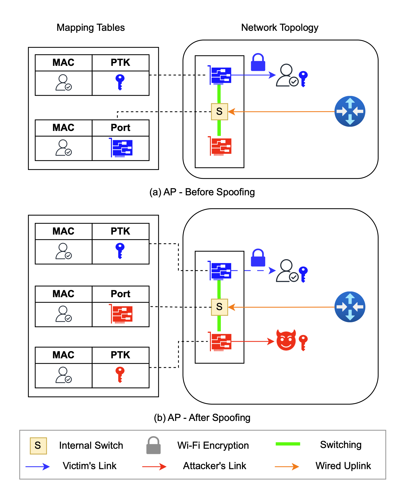


