The world’s first “biological computer” that fuses human brain cells with silicon hardware to form fluid neural networks has been commercially launched, ushering in a new age of AI technology. The CL1, from Australian company Cortical Labs, offers a whole new kind of computing intelligence – one that’s more dynamic, sustainable and energy efficient than any AI that currently exists – and we will start to see its potential when it’s in users’ hands in the coming months.
Known as a Synthetic Biological Intelligence (SBI), Cortical’s CL1 system was officially launched in Barcelona on March 2, 2025, and is expected to be a game-changer for science and medical research. The human-cell neural networks that form on the silicon “chip” are essentially an ever-evolving organic computer, and the engineers behind it say it learns so quickly and flexibly that it completely outpaces the silicon-based AI chips used to train existing large language models (LLMs) like ChatGPT.
“Today is the culmination of a vision that has powered Cortical Labs for almost six years,” said Cortical founder and CEO Dr Hon Weng Chong. “We’ve enjoyed a series of critical breakthroughs in recent years, most notably our research in the journal Neuron, through which cultures were embedded in a simulated game-world, and were provided with electrophysiological stimulation and recording to mimic the arcade game Pong. However, our long-term mission has been to democratize this technology, making it accessible to researchers without specialized hardware and software. The CL1 is the realization of that mission.”
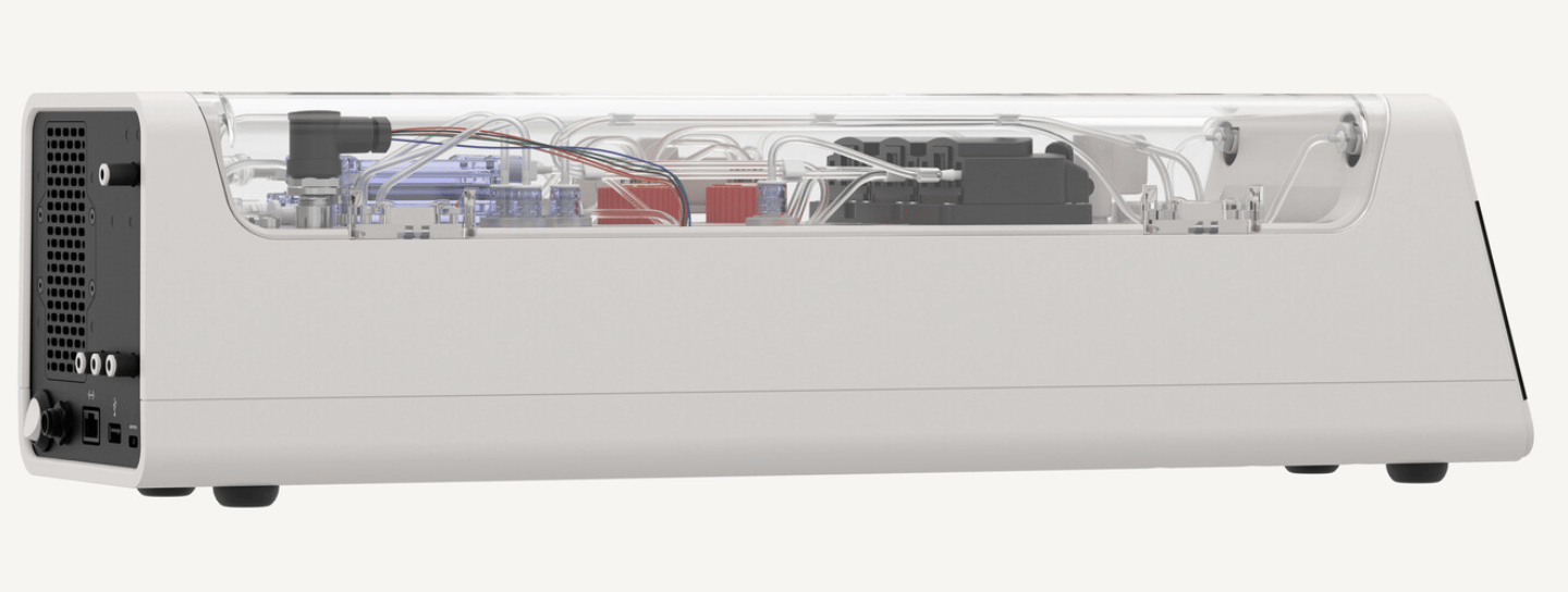
The CL-1: a large housing contains all the life support systems required for the survival of the human brain cells that power the chip
Cortical Labs
He added that while this is a groundbreaking step forward, the full extent of the SBI system won’t be seen until it’s in users’ hands.
“We’re offering ‘Wetware-as-a-Service’ (WaaS),” he added – customers will be able to buy the CL-1 biocomputer outright, or simply buy time on the chips, accessing them remotely to work with the cultured cell technology via the cloud. “This platform will enable the millions of researchers, innovators and big-thinkers around the world to turn the CL1’s potential into tangible, real-word impact. We’ll provide the platform and support for them to invest in R&D and drive new breakthroughs and research.”
These remarkable brain-cell biocomputers could revolutionize everything from drug discovery and clinical testing to how robotic “intelligence” is built, allowing unlimited personalization depending on need. The CL1, which will be widely available in the second half of 2025, is an enormous achievement for Cortical – and as New Atlas saw recently with a visit to the company’s Melbourne headquarters – the potential here is much more far-reaching than Pong.
The team made international headlines in 2022 after developing a self-adapting computer ‘brain’ by placing 800,000 human and mouse neurons on a chip and training this network to play the video game. New Atlas readers may already be familiar with Cortical Labs and its formative steps towards SBI, with Loz Blain covering the early advances of this self-adjusting neural network capable of adjusting and adapting to forge new, stimuli-responsive pathways in processing information.
“We almost view it actually as a kind of different form of life to let’s say, animal or human,” Chief Scientific Officer Brett Kagan told Blain in 2023. “We think of it as a mechanical and engineering approach to intelligence. We’re using the substrate of intelligence, which is biological neurons, but we’re assembling them in a new way.”
Cortical Labs has come a long way since that important first step but now-obsolete DishBrain, both in technology and name. Now, with the commercialization of the CL1, researchers can get hands-on with the the technology, and start exploring a vast range of real-world applications.
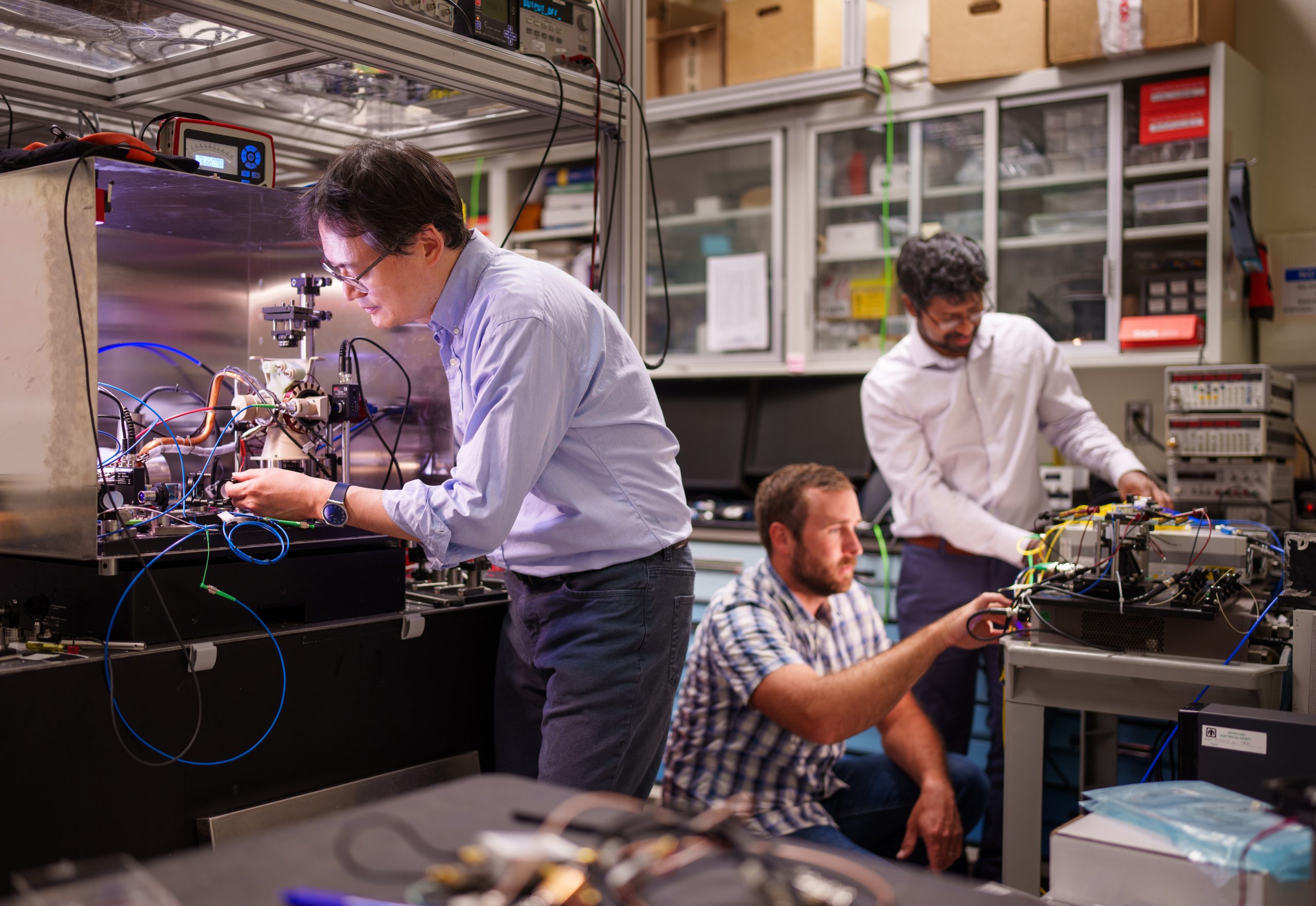
When New Atlas visited Kagan and team at Cortical Labs’ Melbourne headquarters late last year in the lead-up to this launch, we saw first-hand how far the biotechnology has come since the DishBrain. The CL1 features relatively simple, stable hardware, new ways of optimizing “wetware” – human brain cells – and significant strides towards being able to grow a neural network that works like a fully functional brain. Or, as Kagan explained of a work in progress, the “Minimal Viable Brain.”
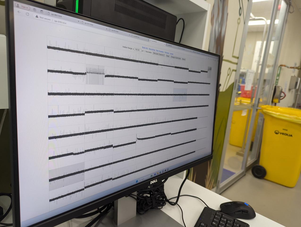
In the lab, the early CL1 model is put through its paces as the team monitors its response to stimuli (prompts)
New Atlas
In 2022, the team demonstrated how rodent- and human-induced pluripotent stem cells (hiPSCs) integrated into high-density multielectrode arrays (HD-MEAs) based on complementary metal–oxide–semiconductor (CMOS) technology could be electro-physiologically stimulated to forge autonomous, highly efficient information-exchange paths.
To do so, they needed a way to reward the brain cells when they exhibited desired behaviors, and punish them when they failed a task. In the DishBrain experiments, they proved that predictability was the key; neurons seek out connections that produce energy-efficient, predictable outcomes and will adapt their networks in search of that reward, while avoiding behaviours that produce a random, chaotic electrical signal.
But, as Kagan explained, that was just the start.
“The current version is totally different technology,” Kagan told Blain and I. “The previous one used something called a CMOS chip, which basically gave you a really high-density read, but it was opaque, you couldn’t see the cells. And there were other issues as well – like, when you stimulate with a CMOS chip, you can’t draw out the charge; you can’t balance the charge as well. You end up with a build-up of charge at where you’re stimulating over long periods of time, and that’s pretty bad for the cells.
“With these versions, they’re a much simpler technology, but that means they’re much more stable and you’re much more able to actively balance that charge,” he added. “When you put in two microamps of current, you can draw out 2 microamps of current. And you can keep it more stable for longer.”
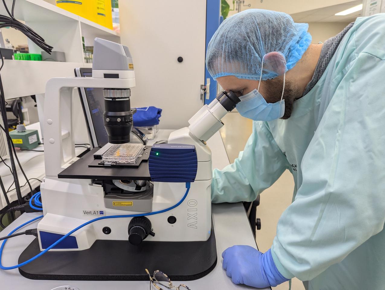
Chief Scientific Officer Brett Kagan assesses some stem cells cultivated in the lab
New Atlas
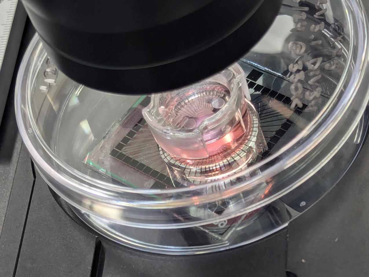
Inside the CL1 system, lab-grown neurons are placed on a planar electrode array – or, as Kagan explained, “basically just metal and glass.” Here, 59 electrodes form the basis of a more stable network, offering the user a high degree of control in activating the neural network. This SBI “brain” is then placed in a rectangular life-support unit, which is then connected to a software-based system to be operated in real time.
“A simple way to describe it would be like a body in a box, but it has filtration for waves, it has where the media is stored, it has pumps to keep everything circulating, gas mixing, and of course temperature control,” Kagan explained.
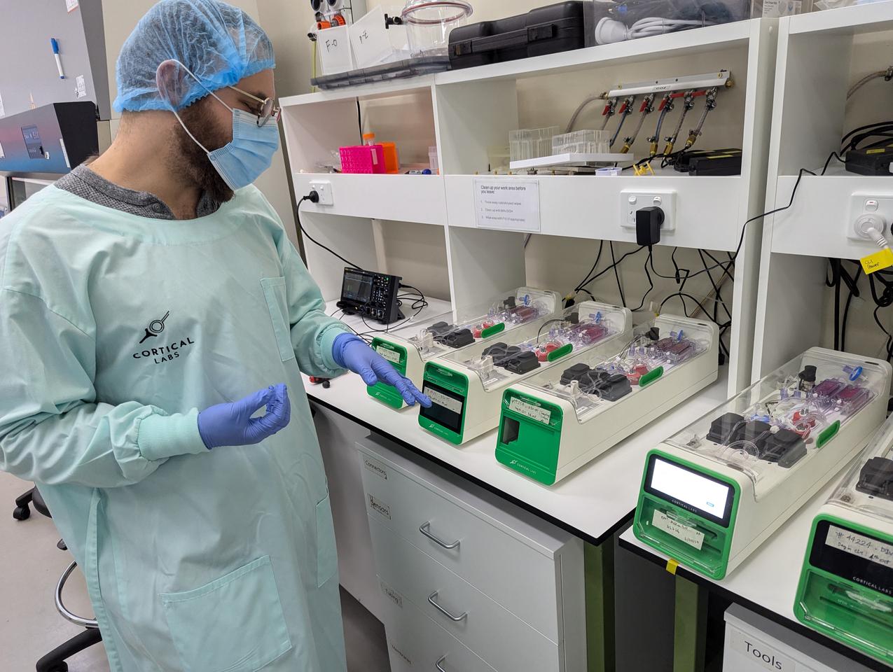
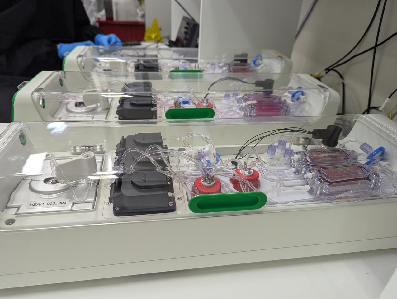
In the lab, Cortical is assembling these units to construct a first-of-its-kind biological neural network server stack, housing 30 individual units that each contain the cells on their electrode array, which is expected to go online in the coming months.
The team aims to have four such stacks running and available for commercial use through a cloud system before the end of the year. The units themselves are expected to have a price tag of around US$35,000, to start with (anything close to this kind of tech is currently priced at €80,000, or nearly US$85,000).
An entire rack of CL1 units uses only around 850-1,000 W of energy, is fully programmable and offers “bi-directional stimulation and read interface, tailored to enable neural communication and network learning,” the team noted in their launch release. Incredibly, the CL1 unit doesn’t require an external computer to operate, either.
Kagan and team testing the CL1 units, which are built to maintain the health of the cells living on the silicon hardware
New Atlas
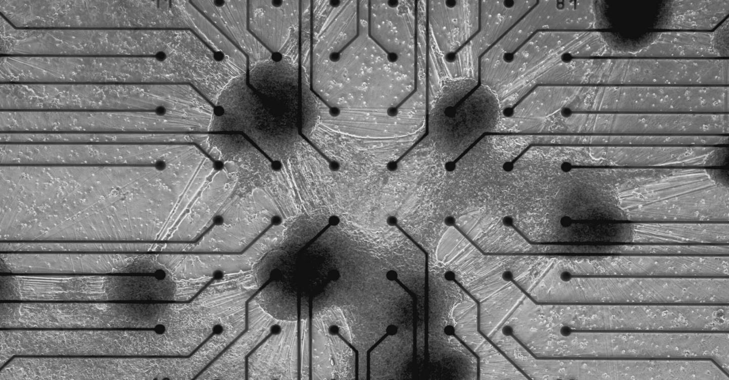
The complex, ever-evolving SBI neural networks – which, under a microscope, can be seen forming branches from electrode to electrode – have, to start with, the potential to revolutionize how drug discovery and disease modeling is researched.
“We’re aiming to be significantly more affordable, and we do want to bring that pricing down in the long-term, but that’s the much longer term,” Kagan said. “In the meantime, we provide access to people from anywhere, anyone, any house, through the cloud-based system.
“So even if you don’t have one of these [units],” he added, “you can access one of these from your home.”
Taking us through the Physical Containment Level, or PC2, laboratory – a mix of computer hardware and more traditional biological specimens and equipment – Kagan showed us some of the all-important induced pluripotent stem cells (IPSC) under the microscope. IPSCs, cultivated in the lab from blood samples, are essentially blank slates that can grow into different types of cells.
“What we do is take those, and we start to use two different methods to differentiate them,” he explained. “One, we can either apply small molecules, which is called an ontogenetic differentiation protocol, where we essentially try to mimic the molecules that happen in utero or, rather, in the foetus’ developing brain. The other method is where we directly differentiate them, where we choose to up-regulate specific genes that are involved in neurons.”
One of the team’s methods is quick and produces a high level of cellular purity, however, the downside is that it isn’t exactly representative of the human brain.
“The brain is not a high-purity organ; it has a lot of different cell types, a lot of different connections,” Kagan said. “So if you only have one cell type, you might have that cell type, but you don’t have a brain.”
Just one section of the CL1 stack, with each unit housing living cells
Cortical Labs
The second method, “the small molecule approach,” produces diverse populations of cells, but it’s often unclear as to exactly what they’re working with. And understanding this is critical to Cortical’s ambitious ongoing pursuit of building the Minimal Viable Brain. While the CL1 launch is the first step, the team is also hard at work on the next stage of SBI.
“You can categorize the main cells, but there’s always a lot of sub-cell types – and that’s really good, as we’ve found out, but we’d really like to have fully controlled direct differentiation,” he explains. “We just haven’t resolved that problem yet: What is the ‘Minimal Viable Brain?’”
The MVB is an intriguing concept: How to bioengineer a human-like “brain” with the least amount of superfluous cell differentiation, but one that would have the complexity that growing a neural network made up of homogenous cell types doesn’t have. This kind of tool would be a powerful model, allowing for even more control and nuanced analyses than what is currently possible in research conducted on a real brain.
“It would basically be the key biological components that allow something to process information in a dynamic and responsive way, according to underlying principles,” Kagan explained. “A single neuron can do a lot of stuff, and while it can respond to some degree of dynamic behavior, it can’t, for example, navigate an environment. The smallest working brains we know of have 301 or 302 – depending on who you ask – neurons, and that’s in the C. elegens. But each of those neurons are really highly specified.
Actual human brain cells, living on a silicon chip among an array of input/output electrodes
Cortical Labs
“And another question is: Is the C. elegens brain the minimal viable brain? Do you need all of those neurons or could you achieve it with, you know, 30 neurons that are all uniquely circuited up?” he continued. (The organism is, of course, the science world’s favorite nematode, Caenorhabditis elegans.)“And if that’s the case, can you build a more complex network of those with 100,000 of the same 30? We don’t know the answer to any of this yet, but with this technology we can uncover it.
“We’re starting to add more and more cell types to this culture as we go, but one thing that’s holding us back is the tools,” he said. “The [CL1] unit didn’t exist until we built it, and you need a tool like that to answer questions like, ‘What is the minimal viable brain?'” If you have 120 units, you can set up really well-controlled experiments to understand exactly what drives the appearance of intelligence. You can break things down to the transcriptomic and genetic level to understand what genes and what proteins is actually driving one to learn and another not to learn. And when you have all those units, you can immediately start to take the drug discovery and disease modeling approach.”
This is particularly important for research into better treatments or even cures for conditions such as epilepsy and Alzheimer’s disease, and other brain-related illnesses. In the meantime, the CL1 system, is expected to advance research into diseases and therapeutics considerably.
“The large majority of drugs for neurological and psychiatric diseases that enter clinical trial testing fail, because there’s so much more nuance when it comes to the brain – but you can actually see that nuance when you test with these tools,” he explained. “Our hope is that we’re able to replace significant areas of animal testing with this. Animal testing is unfortunately still necessary, but I think there are a lot of cases where it can be replaced and that’s an ethically good thing.”
The ethics of this technology has been front and center for Cortical – that breakthrough 2022 paper sparked plenty of debate around it, particularly in the area of human “consciousness” and “sentience.” However, guardrails are in place, as much as they can be, for the ethical use of the CL1 units and the remote WaaS access.
The cells form an entirely new kind of artificial intelligence
New Atlas
“There are numerous regulatory approvals required, based on location and specific use cases,” the team noted in its launch statement. “Regulatory bodies may include health agencies, bioethics committees, and governmental organisations overseeing biotechnology or medical devices. Compliance with these regulations is essential to ensure responsible and ethical use of biological computing technologies.”
But as a global frontrunner in this ambitious technology, Cortical knows that – much like the rapid advancement of non-biological AI – it’s not easy to predict the broad applications of SBI. And one other challenge the company faces is funding – something that the realization of CL1 as a tangible, usable technology might change.
“The difficulty I keep hearing [from investors] is that we don’t fit into a box,” Kagan told us, as we took off our lab coats, hair nets and masks, and relocated to a couch by the computer room upstairs. “And we don’t – we’re a technology that crosses a number of different boundaries. If you look at the priority sectors, we can cover everything from the enabling capabilities of biotechnology, robotics, medical science, and a range of other things. We’re not quite AI, we’re not quite medicine – we can do both AI and medicine, but we’re not either. So we often get excluded.”
The complex life-support system inside each CL1 unit
New Atlas
As such, the launch of the physical CL1 system and the Cortical Cloud for WaaS remote use is a huge achievement, with Kagan and team excited to see where SBI can go once its in people’s hands.
“The CL1 is the first commercialized biological computer, uniquely designed to optimize communication and information processing with in vitro neural cultures,” the team noted. “The CL1, with built-in life support to maintain the health of the cells, holds significant possibilities in the fields of medical science and technology.
“SBI is inherently more natural than AI, as it utilizes the same biological material – neurons – that underpin intelligence in living organisms,” Cortical added. “By leveraging neurons as a computational substrate, SBI has the potential to create systems that exhibit more organic and natural forms of intelligence compared to traditional silicon-based AI.”
[…] The ThinkPad T14s 2-in-1 is by far the most interesting of the bunch, with a new convertible body that’s similar to Lenovo’s Yoga laptops, and supports the magnetic Yoga Pen stylus. The laptop comes with up to a 14-inch, 400-nit WUXGA touch display, and inside, you can get up to a Intel Core Ultra 7 H or U 200 series chip, 64GB of LPDDR5x RAM and 1TB of storage. If you’re looking for an option without a 360-degree hinge, the ThinkPad T14s Gen 6 and ThinkPad T14 Gen 6 will also now come with either Intel Core Ultra or AMD Ryzen AI Pro chips, up to 32GB of RAM and up to 2TB of storage.
Lenovo
Lenovo describes the new ThinkPad X13 Gen 6 as “one of the lightest ThinkPad designs ever,” at only 2.05 lbs, but that light weight doesn’t mean the laptop misses out on the latest internals. The X13 Gen 6 comes with either a Intel Core Ultra or AMD Ryzen AI Pro chip, up to 64GB of LPDDR5x RAM and your choice of a 41Wh or 54.7Wh battery. The new ThinkPad can also support Wi-Fi 7 and an optional 5G connection, if you want to take it on the go.
You might be surprised to learn that the first laptop with built-in solar panels is nearly 15 years old. But to me, the bigger shock is that with all the recent advancements in photovoltaic cells, manufacturers haven’t revisited this idea more often. But at MWC 2025, Lenovo is changing that with its Yoga Solar PC Concept.
Weighing 2.6 pounds and measuring less than 0.6 inches thick, the Yoga Solar PC Concept is essentially the same size as a standard 14-inch clamshell. And because its underlying design isn’t all that different from Lenovo’s standard Yoga family, it doesn’t skimp on specs either. It features an OLED display, up to 32GB of RAM, a decent-sized 50.2 WHr battery and even a 2MP IR webcam for use with Windows Hello.
However, all those components aren’t nearly as important as the solar cells embedded in its lid. Lenovo says the panels use Back Contact Cell technology so that its mounting brackets and gridlines can be placed on the rear of the cells. This allows the panels to offer up to 24 percent solar energy conversion, which is pretty good as that matches the efficiency you get from many high-end home solar systems. Furthermore, the PC also supports Dynamic Solar Tracking to automatically adjust the cells’ settings to maximize the amount of energy they can gather.
1 / 5
Lenovo Yoga Solar PC Concept hands-on photo
Lenovo Yoga Solar PC Concept hands-on photo
Lenovo says this means the Yoga Solar PC can generate enough juice to play an hour of videos after only 20 minutes in the sun. But what might be more impressive is that even when the laptop is indoors, it can still harvest power from as little as 0.3 watts of light to help top off its battery. Finally, to help you understand how much power it’s gathering, Lenovo created a bespoke app to track how much light the panels absorb.
Unfortunately, Lenovo doesn’t have any plans to turn this concept into a full commercial device
In today’s “futuristic tech you can get for $5”, [RealCorebb] shows us a gesture sensor, one of the sci-fi kind. He was doing a desktop clock build, and wanted to add gesture control to it – without any holes that a typical optical sensor needs. After some searching, he’s found Microchip’s MGC3130, a gesture sensing chip that works with “E-fields”, more precise than the usual ones, almost as cheap, and with a lovely twist.
The coolest part about this chip is that it needs no case openings. The 3130 can work even behind obstructions like a 3D-printed case. You do need a PCB the size of a laptop touchpad, however — unlike the optical sensors easy to find from the usual online marketplaces. Still, if you have a spot, this is a perfect gesture-sensing solution. [RealCorebb] shows it off to us in the demo video.
AI hardware startup Humane has given its users just ten (10!) days notice that their Pins will be disconnected. In a note to its customers, the company said AI Pins will “continue to function normally” until 12PM PT on February 28. On that date, users will lose access to essentially all of their device’s features, including but not limited to calling, messaging, AI queries and cloud access. The FAQ does note that you’ll still be able to check on your battery life, though.
Humane is encouraging its users to download any stored data before February 28, as it plans on permanently deleting “all remaining customer data” at the same time as switching its servers off.
[…]
Today’s discontinuation announcement was brought about by the acquisition of Humane by HP, which is buying the company’s intellectual property for $116 million but clearly has no interest in its current hardware business
Today, our mobile phones, computers, and GPS systems can give us very accurate time indications and positioning thanks to the over 400 atomic clocks worldwide. All sorts of clocks — be it mechanical, atomic or a smartwatch — are made of two parts: an oscillator and a counter. The oscillator provides a periodic variation of some known frequency over time while the counter counts the number of cycles of the oscillator. Atomic clocks count the oscillations of vibrating atoms that switch between two energy states with very precise frequency.
Most atomic clocks use microwave frequencies to induce these energy oscillations in atoms. In recent years, researchers in the field have explored the possibility of using laser instead to induce oscillations optically. Just like a ruler with a great number of ticks per centimeter, optical atomic clocks make it possible to divide a second into even more time fractions, resulting in thousands of times more accurate time and position indications.
“Today’s atomic clocks enable GPS systems with a positional accuracy of a few meters. With an optical atomic clock, you may achieve a precision of just a few centimeters.
[…]
The core of the new technology, described in a recently published research article in Nature Photonics, are small, chip-based devices called microcombs. Like the teeth of a comb, microcombs can generate a spectrum of evenly distributed light frequencies.
“This allows one of the comb frequencies to be locked to a laser frequency that is in turn locked to the atomic clock oscillation,” says Minghao Qi.
[…]
the minimal size of the microcomb makes it possible to shrink the atomic clock system significantly while maintaining its extraordinary precision,”
[…]
Another major obstacle has been achieving simultaneously the “self-reference” needed for the stability of the overall system and aligning the microcomb’s frequencies exactly with the atomic clock’s signals.
“It turns out that one microcomb is not sufficient, and we managed to solve the problem by pairing two microcombs, whose comb spacings, i.e. frequency interval between adjacent teeth, are close but with a small offset, e.g. 20 GHz. This 20 GHz offset frequency will serve as the clock signal that is electronically detectable. In this way, we could get the system to transfer the exact time signal from an atomic clock to a more accessible radio frequency, ”
[…]
“Photonic integration technology makes it possible to integrate the optical components of optical atomic clocks, such as frequency combs, atomic sources and lasers, on tiny photonic chips in micrometer to millimeter sizes, significantly reducing the size and weight of the system,” says Dr. Kaiyi Wu.
The innovation could pave the way for mass production, making optical atomic clocks more affordable and accessible for a range of applications in society and science. The system that is required to “count” the cycles of an optical frequency requires many components besides the microcombs, such as modulators, detectors and optical amplifiers. This study solves an important problem and shows a new architecture, but the next steps are to bring all the elements necessary to create a full system on a chip.
Earlier this week, Nvidia confirmed in its official forums that “32-bit CUDA applications are deprecated on GeForce RTX 50 series GPUS.” The company’s support page for its “Support plan for 32-bit CUDA” notes that some 32-bit capabilities were removed from CUDA 12.0 but does not mention PhysX. Effectively, the 50 series cards cannot run any game with PhysX as developers originally intended. That’s ironic, considering Nvidia originally pushed this tech back in the early 2010s to sell its GTX range of GPUs.
PhysX is a GPU-accelerated physics system that allows for more realistic physics simulations in games without putting pressure on the CPU. This included small particle effects like fog or smoke and cloth movement.
[…]
a game like Batman: Arkham City […] with an Nvidia RTX 5070 Ti, and when you try to enable hardware-accelerated physics in settings, you’ll receive a note reading, “Your hardware does not support Nvidia Hardware Accelerated PhysX. Performance will be reduced without dedicated hardware.” [ …] The in-game benchmark shows that with the hardware accelerated physics setting enabled on the RTX 5070 Ti, I saw a hit of 65 average FPS compared to the setting off, from 164 to 99. The difference in ambiance without the setting enabled is striking.
[…]
In other games, like Borderlands 2, it simply grays out the PhysX option in settings. As one Reddit user found, you can force it through editing the game files, but that will result in horrible framerate drops even when shooting a gun at a wall. It’s not what the game makers intended. If you want to play these older games in their prime, your best option is to plug a separate, older GeForce GPU into the system and run 32-bit PhysX games exclusively on that card.
[…]
we see Nvidia deprecating its own hardware capabilities, hurting games that are little more than a decade old
There’s some good news to share for Pebble fans: The no-frills smartwatch is making a comeback. The Vergespoke to Pebble founder Eric Migicovsky today, who says he was able to convince Google to open-source the smartwatch’s operating system. Migicovsky is in the early stages of prototyping a new watch and spinning up a company again under a to-be-announced new name.
Founded back in 2012, Pebble was initially funded on Kickstarter and created smartwatches with e-ink displays that nailed the basics. They could display notifications, let users control their music, and last 5-7 days on a charge thanks to their displays that are akin to what you find on a Kindle. The watches came in at affordable prices too, and they could work across both iOS and Android.
[…]
Fans of Pebble will be happy to know that whatever new smartwatch Migicovsky releases, it will be almost identical to what came before. “We’re building a spiritual, not successor, but clone of Pebble,” he says, “because there’s not that much I actually want to change.” Migicovsky plans to keep the software open-source and allow anyone to customize it for their watches. “There’s going to be the ability for anyone who wants to, to take Pebble source code, compile it, run it on their Pebbles, build new Pebbles, build new watches. They could even use it in random other hardware. Who knows what people can do with it now?”
And of course, this time around Migicovsky is using his own capital to grow the company in a sustainable way. After leaving Pebble, he started a messaging startup called Beeper, which was acquired by WordPress developer Automattic. Migicovsky has also served as an investor at Y-Combinator.
It is unclear when Migicovsky’s first watch may be available, but updates will be shared at rePebble.com.
[…] photonics, which offers lower energy consumption and reduced latency than electronics.
One of the most promising approaches is in-memory computing, which requires the use of photonic memories. Passing light signals through these memories makes it possible to perform operations nearly instantaneously. But solutions proposed for creating such memories have faced challenges such as low switching speeds and limited programmability.
Now, an international team of researchers has developed a groundbreaking photonic platform to overcome those limitations. Their findings were published in the journal Nature Photonics.
[…]
The researchers used a magneto-optical material, cerium-substituted yttrium iron garnet (YIG), the optical properties of which dynamically change in response to external magnetic fields. By employing tiny magnets to store data and control the propagation of light within the material, they pioneered a new class of magneto-optical memories. The innovative platform leverages light to perform calculations at significantly higher speeds and with much greater efficiency than can be achieved using traditional electronics.
This new type of memory has switching speeds 100 times faster than those of state-of-the-art photonic integrated technology. They consume about one-tenth the power, and they can be reprogrammed multiple times to perform different tasks. While current state-of-the-art optical memories have a limited lifespan and can be written up to 1,000 times, the team demonstrated that magneto-optical memories can be rewritten more than 2.3 billion times, equating to a potentially unlimited lifespan.
You can probably complete an amazing number of tasks with your hands without looking at them. But if you put on gloves that muffle your sense of touch, many of those simple tasks become frustrating. Take away proprioception — your ability to sense your body’s relative position and movement — and you might even end up breaking an object or injuring yourself.
[…]
Greenspon and his research collaborators recently published papers in Nature Biomedical Engineering and Science documenting major progress on a technology designed to address precisely this problem: direct, carefully timed electrical stimulation of the brain that can recreate tactile feedback to give nuanced “feeling” to prosthetic hands.
[…]
The researchers’ approach to prosthetic sensation involves placing tiny electrode arrays in the parts of the brain responsible for moving and feeling the hand. On one side, a participant can move a robotic arm by simply thinking about movement, and on the other side, sensors on that robotic limb can trigger pulses of electrical activity called intracortical microstimulation (ICMS) in the part of the brain dedicated to touch.
For about a decade, Greenspon explained, this stimulation of the touch center could only provide a simple sense of contact in different places on the hand.
“We could evoke the feeling that you were touching something, but it was mostly just an on/off signal, and often it was pretty weak and difficult to tell where on the hand contact occurred,” he said.
[…]
By delivering short pulses to individual electrodes in participants’ touch centers and having them report where and how strongly they felt each sensation, the researchers created detailed “maps” of brain areas that corresponded to specific parts of the hand. The testing revealed that when two closely spaced electrodes are stimulated together, participants feel a stronger, clearer touch, which can improve their ability to locate and gauge pressure on the correct part of the hand.
The researchers also conducted exhaustive tests to confirm that the same electrode consistently creates a sensation corresponding to a specific location.
“If I stimulate an electrode on day one and a participant feels it on their thumb, we can test that same electrode on day 100, day 1,000, even many years later, and they still feel it in roughly the same spot,” said Greenspon, who was the lead author on this paper.
[…]
The complementary Science paper went a step further to make artificial touch even more immersive and intuitive. The project was led by first author Giacomo Valle, PhD, a former postdoctoral fellow at UChicago who is now continuing his bionics research at Chalmers University of Technology in Sweden.
“Two electrodes next to each other in the brain don’t create sensations that ’tile’ the hand in neat little patches with one-to-one correspondence; instead, the sensory locations overlap,” explained Greenspon, who shared senior authorship of this paper with Bensmaia.
The researchers decided to test whether they could use this overlapping nature to create sensations that could let users feel the boundaries of an object or the motion of something sliding along their skin. After identifying pairs or clusters of electrodes whose “touch zones” overlapped, the scientists activated them in carefully orchestrated patterns to generate sensations that progressed across the sensory map.
Participants described feeling a gentle gliding touch passing smoothly over their fingers, despite the stimulus being delivered in small, discrete steps. The scientists attribute this result to the brain’s remarkable ability to stitch together sensory inputs and interpret them as coherent, moving experiences by “filling in” gaps in perception.
The approach of sequentially activating electrodes also significantly improved participants’ ability to distinguish complex tactile shapes and respond to changes in the objects they touched. They could sometimes identify letters of the alphabet electrically “traced” on their fingertips, and they could use a bionic arm to steady a steering wheel when it began to slip through the hand.
These advancements help move bionic feedback closer to the precise, complex, adaptive abilities of natural touch, paving the way for prosthetics that enable confident handling of everyday objects and responses to shifting stimuli.
[…]
“We hope to integrate the results of these two studies into our robotics systems, where we have already shown that even simple stimulation strategies can improve people’s abilities to control robotic arms with their brains,” said co-author Robert Gaunt, PhD, associate professor of physical medicine and rehabilitation and lead of the stimulation work at the University of Pittsburgh.
Greenspon emphasized that the motivation behind this work is to enhance independence and quality of life for people living with limb loss or paralysis.
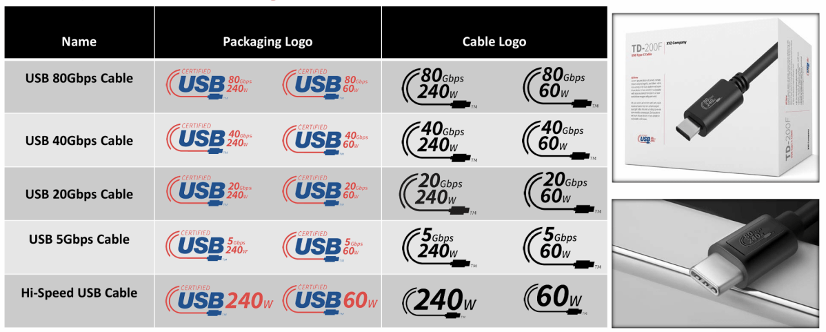
In 2019, the names used by the USB Implementor Forum’s engineering teams to describe the various speeds of USB got leaked, and the backlash (including our own) was harsh. Names like “USB 3.2 Gen 2” mean nothing to consumers — but neither do marketing-style terms, such as “SuperSpeed USB 10Gbps.”
It’s the latter speed-only designation that became the default standard, where users cared less about numerical gobbledygook and more about just how fast a cable was. (Our reviews simply refer to the port by its shape, such as USB-A, and its speed, such as 5Gbps.) In 2022, the USB world settled upon an updated logo scheme that basically cut out everything but the speed of the device or cable.
Thankfully, the USB-IF has taken the extra step and extended its logo scheme to the latest versions of the USB specification, including USB4. It also removes “USB4v2” from consumer branding.
USB-IF
If you’re buying a USB4 or USB4v2 docking station, you’ll simply see a “USB 80Gbps” or “USB 40Gbps” logo on the side of the box now. While it may be a little disconcerting to see a new logo like this, at least you’ll know exactly what you’re buying.
This is a welcome move on several fronts. For one, USB-C ports typically go unlabeled on PCs, so you can’t be sure whether the USB-C port is an older 10Gbps port or a more modern USB4 or Thunderbolt port. (Thunderbolt 4 and USB4v2 are essentially identical, though Intel has its own certification process. Thunderbolt ports aren’t identified by speed, either.) USB-IF representatives told me that they’d heard a rumor that Dell would begin identifying its ports like the primary image above.
The USB-IF is also applying common-sense logos to cables, too, informing users what its throughput and power transmission capabilities are.
Finally, the updated USB logos will also apply to cables. Jeff Ravencraft, president of the USB-IF, said that was done to clearly communicate the only things consumers cared about: what data speeds the cable supported and how much power it could pass between two devices.
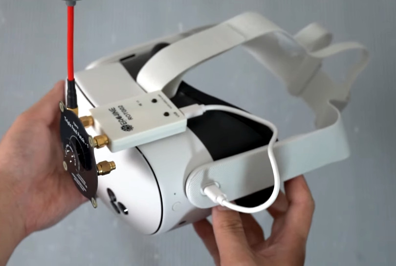
Flying a first-person view (FPV) remote controlled aircraft with goggles is an immersive experience that makes you feel as if you’re really sitting in the cockpit of the plane or quadcopter. Unfortunately, while your wearing the goggles, you’re also completely blind to the world around you. That’s why you’re supposed to have a spotter nearby to keep watch on the local meatspace while you’re looping through the air.
But what if you could have the best of both worlds? What if your goggles not only allowed you to see the video stream from your craft’s FPV camera, but you could also see the world around you. That’s precisely the idea behind mixed reality goggles such as Apple Vision Pro and Meta’s Quest, you just need to put all the pieces together. In a recent video [Hoarder Sam] shows you exactly how to pull it off, and we have to say, the results look quite compelling.
[Sam]’s approach relies on the fact that there’s already cheap analog FPV receivers out there that act as a standard USB video device, with the idea being that they let you use your laptop, smartphone, or tablet as a monitor. But as the Meta Quest 3 is running a fork of Android, these devices are conveniently supported out of the box. The only thing you need to do other than plug them into the headset is head over to the software repository for the goggles and download a video player app.
The FPV receiver can literally be taped to the Meta Quest
With the receiver plugged in and the application running, you’re presented with a virtual display of your FPV feed hovering in front of you that can be moved around and resized. The trick is to get the size and placement of this virtual display down to the point where it doesn’t take up your entire field of vision, allowing you to see the FPV view and the actual aircraft at the same time. Of course, you don’t want to make it too small, or else flying might become difficult.
[Sam] says he didn’t realize just how comfortable this setup would be until he started flying around with it. Obviously being able to see your immediate surroundings is helpful, as it makes it much easier to talk to others and make sure nobody wanders into the flight area. But he says it’s also really nice when bringing your bird in for a landing, as you’ve got multiple viewpoints to work with.
Perhaps the best part of this whole thing is that anyone with a Meta Quest can do this right now. Just buy the appropriate receiver, stick it to your goggles, and go flying. If any readers give this a shot, we’d love to hear how it goes for you in the comments.
Historically, manufacturers have let buyers unlock that access and customize what software their phones run. Notable exceptions in the US have, for the most part, only included carrier-specific phone variants.
Unlocking a Pixel smartphone, for example, requires adjusting a couple of settings and installing a couple of well-known tools. Then you’re ready to purge locked software or install a new launcher. Roughly a year ago, Xiaomi introduced a policy limiting users to three unlocked devices per account, providing only a limited time window for unlocking, and demanding waiting periods before doing so. It’s now gone even further, limiting users to unlocking the bootloader of just a single device throughout the year.
[…]
Custom ROMs usually (but not always) derive from pre-existing OSs like Android or Xiaomi’s HyperOS. To write operating software that works on a certain device, you need to develop it on that specific device. Consequently, individuals and teams throughout the enthusiast phone sphere constantly add to their collections of bootloader-unlocked phones. The new unlocking restrictions could place undue hardship on resource-limited development teams, reducing the number of custom ROMs produced moving forward.
Custom ROMs are not only important so you can do what you want on your hardware, but very important is that they allow you to keep updating a device long beyond manufacturer support (eg Cyanogen mod), keeping “outdated” devices running and useful.
An optical fibre technology can help chips communicate with each other at the speed of light, enabling them to transmit 80 times as much information as they could using traditional electrical connections. That could significantly speed up the training times required for large artificial intelligence models – from months to weeks – while also reducing the energy and emissions costs for data centres.
Most advanced computer chips still communicate using electrical signals carried over copper wires. But as the tech industry races to train large AI models – a process that requires networks of AI superchips to transfer huge amounts of data – companies are eager to link chips using the light-speed communication of fibre optics.
[…]
Khare and his colleagues have developed an optics module that would enable chipmakers to add six times as many optical fibres to the edge of a chip, compared to current technologies. The module uses a structure called an optical waveguide to connect as many as 51 optical fibres per millimetre. It also prevents light signals from one fibre from interfering with its neighbours.
[…]
IBM has already put the optical module through stress tests that included high humidity and temperatures ranging from -40°C (-40°F) to 125°C (257°F). Hutcheson expects that major semiconductor manufacturing companies may be interested in licensing the technology.
For years, car safety experts and everyday drivers have bemoaned the loss of the humble button. Modern cars have almost unilaterally replaced dashboards full of tactile knobs with sleek, iPad-like digital displays, despite concerns these alluring devices might be making distracted driving worse. But there are signs the tide might be shifting.
After going all in on touch screens for years, Korean carmaker Hyundai is publicly shifting gears. Hyundai Design North America Vice President Ha Hak-soo remarked on the shift during a recent interview with JoongAng Daily admitting the company was lured in by the “wow” factor of massive, all-in-one screen-based infotainment systems. Customers apparently didn’t share that enthusiasm.
“When we tested with our focus group, we realized that people get stressed, annoyed and steamed when they want to control something in a pinch but are unable to do so,” Ha said.
Now the company is reversing course. Hyundai previously announced it would use physical buttons and knobs for many in-cabin controls across its new lineup of vehicles. They aren’t alone. Porsche and Volkswagen are amongst the major brands planning to buck the trend. It’s part of what looks like a broader acknowledgment of so-called “screen fatigue” setting in amongst car buyers.
[…]
it turns out drivers, for the most part, aren’t too interested in all that choice and functionality. A survey of U.S. car owners by JD Power last year found a consecutive two-year decline in overall consumer satisfaction with their vehicles for the first time in 28 years. The main driver of that dissatisfaction was complicated, difficult to navigate touch-based infotainment systems. A more recent JD Power survey found that most drivers ranked passenger-side display screens–a growing trend in the industry–as simply “not necessary.” Only 56% of drivers surveyed said they preferred to use their vehicle’s built-in infotainment systems to play audio.
“This year’s study makes it clear that owners find some technologies of little use and/or are continually annoying,” JD Power director of user experience benchmarking and technology Kathleen Rizk, said in a statement.
There’s also evidence a growing reliance on overly complicated touch based infotainment displays may be a safety hazard. A 2017 study conducted by the AAA Foundation claims drivers navigating through in-car screens to program navigation apps and other features were “visually and mentally” distracted for an average of 40 seconds. A car traveling at 50mph could cover half a mile during that time. Buttons and knobs aren’t totally distraction-free, but research shows their tactile response allows drivers to use them more easily without looking down and away from the road. The European New Car Assessment Program (NCAP), an independent safety organization, stepped into the debate earlier this year and announced it would grant five-star safety ratings to cars with physical controls for turn signals, windshield wipers, horns, and other critical features.
If you have Spotify’s soon-to-be-bricked Car Thing, there are a few ways you can give it a new lease on life. YouTuber Dammit Jeff has showcased modifications to Car Thing that makes the device useful as a desktop music controller, customizable shortcut tool, or a simple digital clock. Ars Technica’s Kevin Purdy reports: Spotify had previously posted the code for its uboot and kernel to GitHub, under the very unassuming name “spsgsb” and with no announcement (as discovered by Josh Hendrickson). Jeff has one idea why the streaming giant might not have made much noise about it: “The truth is, this thing isn’t really great at running anything.” It has half a gigabyte of memory, 4GB of internal storage, and a “really crappy processor” (Amlogic S905D2 SoC) and is mostly good for controlling music.
How do you get in? The SoC has a built-in USB “burning mode,” allowing for a connected computer, running the right toolkit, to open up root access and overwrite its firmware. Jeff has quite a few issues getting connected (check his video description for some guidance), but it’s “drag and drop” once you’re in. Jeff runs through a few of the most popular options for a repurposed Car Thing:
– DeskThing, which largely makes Spotify desk-friendly, but adds a tiny app store for weather (including Jeff’s own WeatherWave), clocks, and alternate music controls – GlanceThing, which keeps the music controls but also provides some Stream-Deck-like app-launching shortcuts for your main computer. – Nocturne, currently invite-only, is a wholly redesigned Spotify interface that restores all its Spotify functionality.
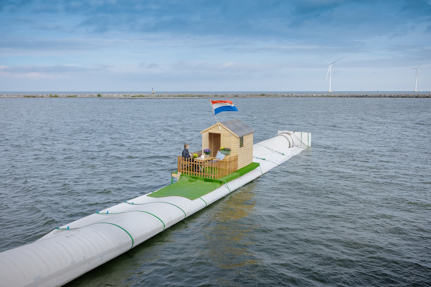
Wind turbines are necessary for ensuring society’s sustainable future, but they still have a recycling problem. Decommissioned installations are destined for landfills in many cases, while the steel parts that actually make it to recycling facilities are only broken down after generating large amounts of (often dirty) greenhouse gas emissions. Two Dutch companies, however, recently proposed new ways to repurpose a wind turbine’s physically largest and most cumbersome pieces into tiny houses, boats, and more.
From October 19 to October 27 at Dutch Design Week 2024, Vattenfall and the design studio Superuse are showcasing a roughly 393-sq-ft home built inside a retired nacelle—the topmost, steel-encased part of a wind turbine containing its generating components such as the generator itself, gearbox, brake train, and drive mechanisms. After hollowing the nacelle of its original internal parts, the team used the casing for a prototype that now features a living space, bathroom, and kitchen with amenities like solar-powered electricity and water heating, as well as a heat pump instead of encasing turbine parts.
Portions of the home interior were also constructed from recycled wind turbine components. Credit: Vattenfall / Jorrit Lousberg Jorrit Lousberg
“We are looking for innovative ways in which you can reuse materials from used turbines… [which necessitates] making something new from them with as few modifications as possible,” Thomas Hjort, Vattenfall’s director of innovation, said in a statement. “That saves raw materials [and] energy consumption, and in this way we ensure that these materials are useful for many years after their first working life.”
Superuse didn’t take the easiest route to the new house. The team—with help from sustainable designing firms Blade-Made and Woodwave—reportedly picked the smallest possible nacelle to construct a building code-compliant dwelling instead of selecting a larger, modern nacelle for the project that would have provided more room for installing electrical wiring and appliances. In this case, the model home uses a V80 2mW turbine’s nacelle. But more recent designs are often much roomier than the 20-year-old V80’s source material, meaning future iterations could provide even more space for inhabitants.
An artists’s conceptualization of an entire community space incorporating recycled wind turbine components. Credit: Courtesy of Vattenfall
The project designers estimate that at least 10,000 V80 turbine nacelles currently exist around the world, most of which are still in operation. That will change in the coming years, however, as global wind energy demands increase and more advanced turbines are installed to fulfill those needs.
“If such a complex structure as a house is possible, then numerous simpler solutions are also feasible and scalable,” argued Jos de Krieger, a partner of Superuse and Blade-Made.
And to make their point, Vattenfall recently offered another example of upcycled turbine parts. Earlier this month, the company also revealed that prototype tests indicate comparatively small turbine blades can be made buoyant with a few modifications. Once properly sealed and reinforced, architects Sonja Draskovic and Jasper Manders topped their 90-foot test blade with green astroturf, an enclosed one-room dwelling, as well as a picket fence and lawn table to demonstrate one use case. And the potential uses for these miniature artificial islands may not end there.
“[W]e started thinking, what can we do with this new land?” Draskovic said in a statement. “Solar parks, playgrounds, houses: anything is possible.”
Other potential uses for wind turbine blades include floating solar farms, traffic noise barriers, and boat houses. Vattenfall / Jorrit Lousberg Jorrit Lousberg
Draskovic and collaborators noted that, like the nacelle home, the blade they used is one of the smallest currently available. More recent designs are nearly 328-feet-long, which may present challenges in future float tests. But blade repurposing doesn’t need to stick to the seas. Aside from boats, designers believe decommissioned turbine blades or their smaller parts may find their way into traffic noise barriers or parking garages.
It will likely take a combination of reuses to fully complete a wind turbine’s circular life cycle, while especially problematic components such as their rare earth element-laden batteries require additional consideration and solutions. Meanwhile, the design teams still need to perform additional experiments and alterations on both the tiny home and boat before scaling them for wider use. Still, the recycling prompts have already inspired people like Vattenhall’s director of innovation to look to the future for additional recycling possibilities.
“With this design, I no longer see images of wind turbine blades that we bury underground like bulky waste,” Thomas said.
Microsoft has removed Windows Mixed Reality from Windows 11.
With Windows 11 24H2, the latest major version of Microsoft’s PC operating system, you can no longer use a Windows MR headset in any way – not even on Steam.
This includes all the Windows MR headsets from Acer, Asus, Dell, HP, Lenovo, and Samsung, including HP’s Reverb G2, released in 2020.
Screenshot taken by UploadVR.
UploadVR tested Windows 11 24H2 with a Reverb G2 and found the above notice. Microsoft confirmed to UploadVR that this is an intentional removal when it originally announced the move back in December.
In August 3.49% of SteamVR users were using a Windows MR headset, which we estimate to be around 80,000 people. If they install Windows 11 24H2, their VR headset will effectively become a paperweight.
“Existing Windows Mixed Reality devices will continue to work with Steam through November 2026, if users remain on their current released version of Windows 11 (version 23H2) and do not upgrade to this year’s annual feature update for Windows 11 (version 24H2).”
The death of Windows MR headsets comes on the same week Microsoft revealed that HoloLens 2 production has ended, and that software support for the AR headset will end after 2027.
Despite the name, all Windows MR headsets were actually VR-only, and are compatible with most SteamVR content via Microsoft’s SteamVR driver.
The first Windows MR headsets arrived in late 2017 from Acer, Asus, Dell, HP, Lenovo, and Samsung, aiming to compete with the Oculus Rift and HTC Vive that had launched a year earlier. They were the first consumer VR products to deliver inside-out positional tracking, for both the headset and controllers.
[…]
In recent years Microsoft has shifted its XR focus to a software-based long term strategic partnership with Meta.
Soon, it will also bring automatic extension of Windows 11 laptops by just looking at them, including spawning entirely virtual extra monitors.
And earlier this year Microsoft announced Windows Volumetric Apps, a new API for extending 3D elements of PC applications being streamed to Meta Quest into 3D space.
A real crying shame. So another reason people will hang on to their Windows 10 installations even more. Hopefully (but doubtfully) they will release the source code and allow people to chug on under their own steam. Bricking these headsets in under four years should be illegal.
Consumer and digital rights activists are calling on the US Federal Trade Commission to stop device-makers using software to reduce product functionality, bricking unloved kit, or adding surprise fees post-purchase.
In an eight-page letter [PDF] to the Commission (FTC), the activists mentioned the Google/Levis collaboration on a denim jacket that contained sensors enabling it to control an Android device through a special app. When the app was discontinued in 2023, the jacket lost that functionality. The letter also mentions the “Car Thing,” an automotive infotainment device created by Spotify, which bricked the device fewer than two years after launch and didn’t offer a refund.
Another example highlighted is the $1,695 Snoo connected bassinet, manufactured by an outfit named Happiest Baby. Kids outgrow bassinets, yet Happiest Baby this year notified customers that if they ever sold or gave away their bassinets, the device’s next owner would have to pay a new $19.99 monthly subscription fee to keep certain features. Activists argue that reduces the resale value of the devices.
Signatories to the letter include individuals from Consumer Reports, the Electronic Frontier Foundation, teardown artists iFixit, and the Software Freedom Conservancy. Environmental groups and computer repair shops also signed the letter.
The signatories urged the FTC to create “clear guidance” that would prevent device manufacturers from using software that locks out features and functions in products that are already owned by customers.
The practice of using software to block features and functions is referred to by the signatories as “software tethering.”
“Consumers need a clear standard for what to expect when purchasing a connected device,” stated Justin Brookman, director of technology policy at Consumer Reports and a former policy director of the FTC’s Office of Technology, Research, and Investigation. “Too often, consumers are left with devices that stop functioning because companies decide to end support without little to no warning. This leaves people stranded with devices they once relied on, unable to access features or updates.”
“Consumers increasingly face a death by a thousand cuts as connected products they purchase lose their software support or advertised features that may have prompted the original purchase,” the letter states. “They may see the device turned into a brick or their favorite features locked behind a subscription. Such software tethers also prevent consumers from reselling their purchases, as some software features may not transfer, or manufacturers may shut down devices, causing a second-hand buyer harm.”
More recent examples are Anova suddenly charging for a subscription, Peloton suddenly asking for an extra fee for resold units. In the past the field is long and littered, with video games being orphaned being pretty huge, but many many gadget makers (Logitech is really good at this) abandoning products and bricking them.
Researchers at Cornell University tapped into fungal mycelia to power a pair of proof-of-concept robots. Mycelia, the underground fungal network that can sprout mushrooms as its above-ground fruit, can sense light and chemical reactions and communicate through electrical signals. This makes it a novel component in hybrid robotics that could someday detect crop conditions otherwise invisible to humans.
The Cornell researchers created two robots: a soft, spider-like one and a four-wheeled buggy. The researchers used mycelia’s light-sensing abilities to control the machines using ultraviolet light. The project required experts in mycology (the study of fungi), neurobiology, mechanical engineering, electronics and signal processing.
“If you think about a synthetic system — let’s say, any passive sensor — we just use it for one purpose,” lead author Anand Mishra said. “But living systems respond to touch, they respond to light, they respond to heat, they respond to even some unknowns, like signals. That’s why we think, OK, if you wanted to build future robots, how can they work in an unexpected environment? We can leverage these living systems, and any unknown input comes in, the robot will respond to that.”
The fungal robot uses an electrical interface that (after blocking out interference from vibrations and electromagnetic signals) records and processes the mycelia’s electrophysical activity in real time. A controller, mimicking a portion of animals’ central nervous systems, acted as “a kind of neural circuit.” The team designed the controller to read the fungi’s raw electrical signal, process it and translate it into digital controls. These were then sent to the machine’s actuators.
Cornell University / Science Robotics
The pair of shroom-bots successfully completed three experiments, including walking and rolling in response to the mycelia’s signals and changing their gaits in response to UV light. The researchers also successfully overrode the mycelia’s signals to control the robots manually, a crucial component if later versions were to be deployed in the wild.
researchers from Sandia National Laboratories have used silicon photonic microchip components to perform a quantum sensing technique called atom interferometry, an ultra-precise way of measuring acceleration. It is the latest milestone toward developing a kind of quantum compass for navigation when GPS signals are unavailable.
Sandia National Laboratories scientist Jongmin Lee, left, prepares a rubidium cold-atom cell for an atom interferometry experiment while scientists Ashok Kodigala, right, and Michael Gehl initialize the controls for a packaged single-sideband modulator chip. Credit: Craig Fritz, Sandia National Laboratories
The team published its findings and introduced a new high-performance silicon photonic modulator — a device that controls light on a microchip — as the cover story in the journal Science Advances.
[…]
Typically, an atom interferometer is a sensor system that fills a small room. A complete quantum compass — more precisely called a quantum inertial measurement unit — would require six atom interferometers.
But Lee and his team have been finding ways to reduce its size, weight, and power needs. They already have replaced a large, power-hungry vacuum pump with an avocado-sized vacuum chamber and consolidated several components usually delicately arranged across an optical table into a single, rigid apparatus.
The new modulator is the centerpiece of a laser system on a microchip. Rugged enough to handle heavy vibrations, it would replace a conventional laser system typically the size of a refrigerator.
Lasers perform several jobs in an atom interferometer, and the Sandia team uses four modulators to shift the frequency of a single laser to perform different functions.
However, modulators often create unwanted echoes called sidebands that need to be mitigated.
Sandia’s suppressed-carrier, single-sideband modulator reduces these sidebands by an unprecedented 47.8 decibels — a measure often used to describe sound intensity but also applicable to light intensity — resulting in a nearly 100,000-fold drop.
[…]
“Just one full-size single-sideband modulator, a commercially available one, is more than $10,000,” Lee said.
Miniaturizing bulky, expensive components into silicon photonic chips helps drive down these costs.
“We can make hundreds of modulators on a single 8-inch wafer and even more on a 12-inch wafer,” Kodigala said.
And since they can be manufactured using the same process as virtually all computer chips, “This sophisticated four-channel component, including additional custom features, can be mass-produced at a much lower cost compared to today’s commercial alternatives, enabling the production of quantum inertial measurement units at a reduced cost,” Lee said.
As the technology gets closer to field deployment, the team is exploring other uses beyond navigation. Researchers are investigating whether it could help locate underground cavities and resources by detecting the tiny changes these make to Earth’s gravitational force. They also see potential for the optical components they invented, including the modulator, in LIDAR, quantum computing, and optical communications.
Researchers from North Carolina State University and Johns Hopkins University have demonstrated a technology capable of a suite of data storage and computing functions—repeatedly storing, retrieving, computing, erasing or rewriting data—that uses DNA rather than conventional electronics. Previous DNA data storage and computing technologies could complete some but not all of these tasks.
The paper, titled “A Primordial DNA Store and Compute Engine,” appears in the journal Nature Nanotechnology.
[…]
“DNA computing has been grappling with the challenge of how to store, retrieve and compute when the data is being stored in the form of nucleic acids,”
[…]
we have created polymer structures that we call dendricolloids—they start at the microscale, but branch off from each other in a hierarchical way to create a network of nanoscale fibers,
[…]
“This morphology creates a structure with a high surface area, which allows us to deposit DNA among the nanofibrils without sacrificing the data density that makes DNA attractive for data storage in the first place.”
“You could put a thousand laptops’ worth of data into DNA-based storage that’s the same size as a pencil eraser,” Keung says.
“The ability to distinguish DNA information from the nanofibers it’s stored on allows us to perform many of the same functions you can do with electronic devices,”
[…]
“We can copy DNA information directly from the material’s surface without harming the DNA. We can also erase targeted pieces of DNA and then rewrite to the same surface, like deleting and rewriting information stored on the hard drive. It essentially allows us to conduct the full range of DNA data storage and computing functions. In addition, we found that when we deposit DNA on the dendricolloid material, the material helps to preserve the DNA.”
The first reports of instability issues with the 13th-gen Intel desktop CPUs started popping up in late 2022, mere months after the models came out. Those issues persisted, and over time, users reported dealing with unexpected and sudden crashes on PCs equipped with the company’s 14th-gen CPUs, as well. Now, Intel has announced that it finally found the reason why its 13th and 14th-gen desktop processors have been causing crashes and giving out on users, and it promises to roll out a fix by next month.
In its announcement, Intel said that based on extensive analysis of the processors that had been returned to the company, it has determined that elevated operating voltage was causing the instability issues. Apparently, it’s because a microcode algorithm — microcodes, or machine codes, are sets of hardware-level instructions — has been sending incorrect voltage requests to the processor.
Intel has now promised to release a microcode patch to address the “root cause of exposure to elevated voltages.” The patch is still being validated to ensure that it can address all “scenarios of instability reported to Intel,” but the company is aiming to roll it out by mid-August.
As wccftech notes, while Intel’s CPUs have been causing issues with users for at least a year and a half, a post on X by Sebastian Castellanos in February put the problem in the spotlight. Castellanos wrote that there was a “worrying trend” of 13th and 14th-gen Intel CPUs having stability issues with Unreal Engine 4 and 5 games, such as Fortnite and Hogwarts Legacy. He also noticed that the issue seems to affect mostly higher-end models and linked to a discussion on Steam Community. The user that wrote the post on Steam wanted to issue a warning to those experiencing “out of video memory trying to allocate a rendering resource” errors that it was their CPU that was faulty. They also linked to several Reddit threads with people experiencing the same problem and who had determined that their issue lied with their Intel CPUs.
More recently, the indie studio Alderon Games published a post about “encountering significant problems with Intel CPU stability” while developing its multiplayer dinosaur survival game Path of Titans. Its founder, Matthew Cassells, said the studio found that the issue affected end customers, dedicated game servers, developers’ computers, game server providers and even benchmarking tools that use Intel’s 13th and 14th-gen CPUs. Cassells added that even the CPUs that initially work well deteriorate and eventually fail, based on the company’s observations. “The failure rate we have observed from our own testing is nearly 100 percent,” the studio’s post reads, “indicating it’s only a matter of time before affected CPUs fail.”
Modern graphics cards use lots of power and all of it is turned into heat. So if you’re paying many hundreds of dollars for a powerful GPU, you’d expect no expense to be spared on the cooling system. It turns out that for many Nvidia RTX 40-series vendors, the expense is being spared and cheap, poorly applied thermal paste is leading to scorching high hotspot temperatures and performance degradation over time.
That’s the conclusion hardware tester Igor’s Lab has come to after testing multiple GeForce RTX cards, analysing temperatures and performance, and discovering that the thermal paste used by many graphics card vendors is not only sub-standard for the job but is also poorly applied.
I have four RTX 40-series cards in my office (RTX 4080 Super, 4070 Ti, and two 4070s) and all of them have quite high hotspots—the highest temperature recorded by an individual thermal sensor in the die. In the case of the 4080 Super, it’s around 11 °C higher than the average temperature of the chip. I took it apart to apply some decent quality thermal paste and discovered a similar situation to that found by Igor’s Lab.
In the space of a few months, the factory-applied paste had separated and spread out, leaving just an oily film behind, and a few patches of the thermal compound itself. I checked the other cards and found that they were all in a similar state.
[…]
Removing the factory-installed paste from another RTX 4080 graphics card, Igor’s Lab applied a more appropriate amount of a high-quality paste and discovered that it lowered the hotspot temperature by nearly 30 °C.
But it’s not just about the hotspots. Cheap, poorly applied thermal paste will cause the performance of a graphics card to degrade over time because GPUs lower clock speeds when they reach their thermal limits. PC enthusiasts are probably very comfortable with replacing a CPU’s thermal paste regularly but it’s not a simple process with graphics cards.
[…]
While Nvidia enjoys huge margins on its GPUs, graphics card vendors aren’t quite so lucky, but they’re not so small that spending a few more dollars on better thermal paste isn’t going to bankrupt the company.
Mind you, if they all started using PTM7950, then none of this would be an issue—the cards would run cooler and would stay that way for much longer. The only problem then is that you’d hear the coil whine over the reduced fan noise.
“Intel’s problems with unstable 13th-gen and 14th-gen high-end CPUs appear to run deeper than we thought,” writes TechRadar, “and a new YouTube video diving into these gremlins will do little to calm any fears that buyers of Raptor Lake Core i9 processors (and its subsequent refresh) have.” Level1Techs is the YouTuber in question, who has explored several avenues in an effort to make more sense of the crashing issues with these Intel processors that are affecting some PC gamers and making their lives a misery — more so in some cases than others. Data taken from game developer crash logs — from two different games — clearly indicates a high prevalence of crashes with the mentioned more recent Intel Core i9 chips (13900K and 14900K).
In fact, for one particular type of error (decompression, a commonly performed operation in games), there was a total of 1,584 that occurred in the databases Level1Techs sifted through, and an alarming 1,431 of those happened with a 13900K or 14900K. Yes — that’s 90% of those decompression errors hitting just two specific CPUs. As for other processors, the third most prevalent was an old Intel Core i7 9750H (Coffee Lake laptop CPU) — which had a grand total of 11 instances. All AMD processors in total had just 4 occurrences of decompression errors in these game databases. “In case you were thinking that AMD chips might be really underrepresented here, hence that very low figure, well, they’re not — 30% of the CPUs in the database were from Team Red…”
“The YouTuber also brings up another point here: namely that data centers are noticing these issues with Core i9s.”