Last week we wrote about a lawsuit against Western Digital that alleged that the firm’s solid state drive didn’t live up to its marketing promises. More lawsuits have been filed against the company since. ArsTechnica: On Thursday, two more lawsuits were filed against Western Digital over its SanDisk Extreme series and My Passport portable SSDs. That brings the number of class-action complaints filed against Western Digital to three in two days. In May, Ars Technica reported about customer complaints that claimed SanDisk Extreme SSDs were abruptly wiping data and becoming unmountable. Ars senior editor Lee Hutchinson also experienced this problem with two Extreme SSDs. Western Digital, which owns SanDisk, released a firmware update in late May, saying that currently shipping products weren’t impacted. But the company didn’t mention customer complaints of lost data, only that drives could “unexpectedly disconnect from a computer.”
Further, last week The Verge claimed a replacement drive it received after the firmware update still wiped its data and became unreadable, and there are some complaints on Reddit pointing to recent problems with Extreme drives. All three cases filed against Western Digital this week seek class-action certification (Ars was told it can take years for a judge to officially state certification and that cases may proceed with class-wide resolutions possibly occurring before official certification). Ian Sloss, one of the lawyers representing Matthew Perrin and Brian Bayerl in a complaint filed yesterday, told Ars he doesn’t believe class-action certification will be a major barrier in a case “where there is a common defect in the firmware that is consistent in all devices.” He added that defect cases are “ripe for class treatment.”
German semiconductor maker Infineon Technologies AG announced that it’s producing a printed circuit board (PCB) that dissolves in water. Sourced from UK startup Jiva Materials, the plant-based Soluboard could provide a new avenue for the tech industry to reduce e-waste as companies scramble to meet climate goals by 2030.
Jiva’s biodegradable PCB is made from natural fibers and a halogen-free polymer with a much lower carbon footprint than traditional boards made with fiberglass composites. A 2022 study by the University of Washington College of Engineering and Microsoft Research saw the team create an Earth-friendly mouse using a Soluboard PCB as its core. The researchers found that the Soluboard dissolved in hot water in under six minutes. However, it can take several hours to break down at room temperature.
In addition to dissolving the PCB fibers, the process makes it easier to retrieve the valuable metals attached to it. “After [it dissolves], we’re left with the chips and circuit traces which we can filter out,” said UW assistant professor Vikram Iyer, who worked on the mouse project.
[…]
Jiva says the board has a 60 percent smaller carbon footprint than traditional PCBs — specifically, it can save 10.5 kg of carbon and 620 g of plastic per square meter of PCB.
Today, the Institute of Electrical and Electronics Engineers (IEEE) has added 802.11bb as a standard for light-based wireless communications. The publishing of the standard has been welcomed by global Li-Fi businesses, as it will help speed the rollout and adoption of the data-transmission technology standard.
Advantages of using light rather than radio frequencies (RF) are highlighted by Li-Fi proponents including pureLiFi, Fraunhofer HHI, and the Light Communications 802.11bb Task Group. Li-Fi is said to deliver “faster, more reliable wireless communications with unparalleled security compared to conventional technologies such as Wi-Fi and 5G.” Now that the IEEE 802.11bb Li-Fi standard has been released, it is hoped that interoperability between Li-Fi systems with the successful Wi-Fi will be fully addressed.
[…]
Where Li-Fi shines (pun intended) is not just in its purported speeds as fast as 224 GB/s. Fraunhofer’s Dominic Schulz points out that as it works in an exclusive optical spectrum, this ensures higher reliability and lower latency and jitter. Moreover “Light’s line-of-sight propagation enhances security by preventing wall penetration, reducing jamming and eavesdropping risks, and enabling centimetre-precision indoor navigation,” says Shultz.
[…]
One of the big wheels of Li-Fi, pureLiFi, has already prepared the Light Antenna ONE module for integration into connected devices.
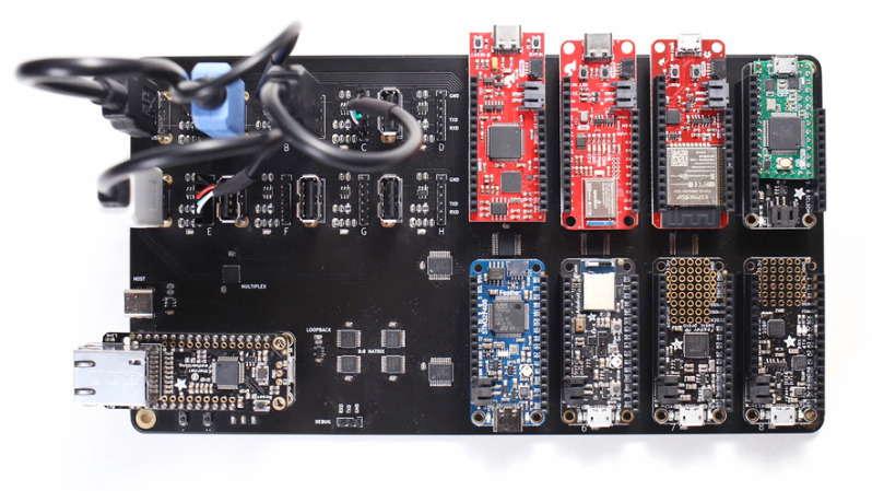
The concept of Continuous Integration (CI) is a powerful tool in software development, and it’s not every day we get a look at how someone integrated automated hardware testing into their system. [Michael Orenstein] brought to our attention the Hardware CI Arena, a framework for doing exactly that across a variety of host OSes and microcontroller architectures.
[…]
The Hardware CI Arena (GitHub repository) was created to allow automated testing to be done across a variety of common OS and hardware configurations. It does this by allowing software-controlled interactions to a bank of actual, physical hardware options. It’s purpose-built for a specific need, but the level of detail and frank discussion of the issues involved is an interesting look at what it took to get this kind of thing up and running.
The value of automatic hardware testing with custom rigs is familiar ground to anyone who develops hardware, but tying that idea into a testing and CI framework for a software product expands the idea in a useful way. When it comes to identifying problems, earlier is always better.
When should you be concerned about a NAS hard drive failing? Multiple factors are at play, so many might turn to various SMART (self-monitoring, analysis, and reporting technology) data. When it comes to how long the drive has been active, there are backup companies like Backblaze using hard drives that are nearly 8 years old. That may be why some customers have been panicked, confused, and/or angered to see their Western Digital NAS hard drive automatically given a warning label in Synology’s DiskStation Manager (DSM) after they were powered on for three years. With no other factors considered for these automatic flags, Western Digital is accused of age-shaming drives to push people to buy new HDDs prematurely.
The practice’s revelation is the last straw for some users. Western Digital already had a steep climb to win back NAS customers’ trust after shipping NAS drives with SMR (shingled magnetic recording) instead of CMR (conventional magnetic recording). Now, some are saying they won’t use or recommend the company’s hard drives anymore.
“Warning,” your NAS drive’s been on for 3 years
As users have reported online, including on Synology-focused and Synology’s ownforums, as well as on Reddit and YouTube, Western Digital drives using Western Digital Device Analytics (WDDA) are getting a “warning” stamp in Synology DSM once their power-on hours count hits the three-year mark. WDDA is similar to SMART monitoring and rival offerings, like Seagate’s IronWolf, and is supposed to provide analytics and actionable items.
The recommended action says: “The drive has accumulated a large number of power on hours [throughout] the entire life of the drive. Please consider to replace the drive soon.” There seem to be no discernible problems with the hard drives otherwise.
Synology confirmed this to Ars Technica and noted that the labels come from Western Digital, not Synology. A spokesperson said the “WDDA monitoring and testing subsystem is developed by Western Digital, including the warning after they reach a certain number of power-on-hours.”
The practice has caused some, like YouTuber SpaceRex, to stop recommending Western Digital drives for the foreseeable future. In May, the YouTuber and tech consultant described his outrage, saying three years is “absolutely nothing” for a NAS drive and lamenting the flags having nothing to do with anything besides whether or not a drive has been in use for three years.
[…]
Users are also concerned that this could prevent people from noticing serious problems with their drive.
Further, you can’t repair a pool with a drive marked with a warning label.
“Only drives with a healthy status can be used to repair or expand a storage pool,” Synology’s spokesperson said. “Users will need to first suppress the warning or disable WDDA to continue.”
[…]
Since Western Digital’s questionable practice has come to light, there has been discussion about how to disable WDDA via SSH.
Synology’s spokesperson said if WDDA is enabled in DSM, one could disable WDDA in Storage Manager and see the warning removed.
“Because the warning is triggered by a fixed power-on-hour count, we do not believe [disabling WDDA] it to be a risk. However, administrators should still pay close attention to their systems, including if other warnings or I/O disruptions occur,” the Synology rep said. “Indicators such as significantly slower reads/writes are more evident signs that a drive’s health may be deteriorating.”
A US federal court this week gave final approval to the $50 million class-action settlement Apple came to last July resolving claims the company knew about and concealed the unreliable nature of keyboards on MacBook, MacBook Air and MacBook Pro computers released between 2015 and 2019. Per Reuters (via 9to5Mac), Judge Edward Davila on Thursday called the settlement involving Apple’s infamous “butterfly” keyboards “fair, adequate and reasonable.” Under the agreement, MacBook users impacted by the saga will receive settlements between $50 and $395. More than 86,000 claims for class member payments were made before the application deadline last March, Judge Davila wrote in his ruling.
Apple debuted the butterfly keyboard in 2015 with the 12-inch MacBook. At the time, former design chief Jony Ive boasted that the mechanism would allow the company to build ever-slimmer laptops without compromising on stability or typing feel. As Apple re-engineered more of its computers to incorporate the butterfly keyboard, Mac users found the design was susceptible to dust and other debris. The company introduced multiple revisions to make the mechanism more resilient before eventually returning to a more conventional keyboard design with the 16-inch MacBook Pro in late 2019.
Some HP “Officejet” printers can disable this “dynamic security” through a firmware update, PC World reported earlier this week. But HP still defends the feature, arguing it’s “to protect HP’s innovations and intellectual property, maintain the integrity of our printing systems, ensure the best customer printing experience, and protect customers from counterfeit and third-party ink cartridges that do not contain an original HP security chip and infringe HP’s intellectual property.”
Meanwhile, Engadget now reports that “a software update Hewlett-Packard released earlier this month for its OfficeJet printers is causing some of those devices to become unusable.” After downloading the faulty software, the built-in touchscreen on an affected printer will display a blue screen with the error code 83C0000B. Unfortunately, there appears to be no way for someone to fix a printer broken in this way on their own, partly because factory resetting an HP OfficeJet requires interacting with the printer’s touchscreen display. For the moment, HP customers report the only solution to the problem is to send a broken printer back to the company for service. BleepingComputer says the firmware update “has been bricking HP Office Jet printers worldwide since it was released earlier this month…” “Our teams are working diligently to address the blue screen error affecting a limited number of HP OfficeJet Pro 9020e printers,” HP told BleepingComputer… Since the issues surfaced, multiple threads have been started by people from the U.S., the U.K., Germany, the Netherlands, Australia, Poland, New Zealand, and France who had their printers bricked, some with more than a dozen pages of reports.
“HP has no solution at this time. Hidden service menu is not showing, and the printer is not booting anymore. Only a blue screen,” one customer said.
“I talked to HP Customer Service and they told me they don’t have a solution to fix this firmware issue, at the moment,” another added.
Hewlett-Packard, or HP, has sparked fury after issuing a recent “firmware” update which blocks customers from using cheaper, non-HP ink cartridges in its printers.
Customers’ devices were remotely updated in line with new terms which mean their printers will not work unless they are fitted with approved ink cartridges.
It prevents customers from using any cartridges other than those fitted with an HP chip, which are often more expensive. If the customer tries to use a non-HP ink cartridge, the printer will refuse to print.
HP printers used to display a warning when a “third-party” ink cartridge was inserted, but now printers will simply refuse to print altogether.
[…]
This is not the first time HP has angered its customers by blocking the use of other ink cartridges.
The firm has been forced to pay out millions in compensation to customers in America, Australia and across Europe since it first introduced dynamic security measures back in 2016.
Just last year the company paid $1.35m (£1m) to consumers in Belgium, Italy, Spain and Portugal who had bought printers not knowing they were equipped with the cartridge-blocking feature.
Last year consumer advocates called on the Competition and Markets Authority to investigate whether branded ink costs and “dynamic security” measures were fair to consumers, after finding that lesser-known brands of ink cartridges offered better value for money than major names.
The consumer group Which? said manufacturers were “actively blocking customers from exerting their right to choose the cheapest ink and therefore get a better deal”.
Samsung Electronics has been stung for more than $303 million in a patent infringement case brought by US memory company Netlist.
Netlist, headquartered in Irvine, California, styles itself as a provider of high-performance modular memory subsystems. The company initially filed a complaint that Samsung had infringed on three of its patents, later amended to six [PDF]. Following a six-day trial, the jury found for Netlist in five of these and awarded a total of $303,150,000 in damages.
The exact patents in question are 10,949,339 (‘339), 11,016,918 (‘918), 11,232,054 (‘054), 8,787,060 (‘060), and 9,318,160 (‘160). The products that are said to infringe on these are Samsung’s DDR4 LRDIMM, DDR5 UDIMM, SODIMM, and RDIMM, plus the high-bandwidth memory HBM2, HBM2E and HBM3 technologies.
The patents appear to apply to various aspects of DDR memory modules. According to reports, Samsung’s representatives had argued that Netlist’s patents were invalid because they were already covered by existing technology and that its own memory chips did not function in the same way as described by the patents, but this clearly did not sway the jurors.
However, it appears that the verdict did not go all Netlist’s way because its lawyers had been arguing for more damages, saying that a reasonable royalty figure would be more like $404 million.
In the court filings [PDF], Netlist claims that Samsung had knowledge of the patents in question “no later than August 2, 2021” via access to Netlist’s patent portfolio docket.
The company states that Samsung and Netlist were initially partners under a 2015 Joint Development and License Agreement (JDLA), which granted Samsung a five-year paid-up license to Netlist’s patents.
Samsung had used Netlist’s technologies to develop products such as DDR4 memory modules and emerging new technologies, including DDR5 and HBM, Netlist said.
Under the terms of the agreement, Samsung was to supply Netlist certain memory products at competitive prices, but Netlist claimed Samsung repeatedly failed to honor these promises. As a result, Netlist claims, it terminated the JDLA on July 15, 2020.
Netlist alleged in its court filing that Samsung has continued to make and sell memory products “with materially the same structures” as those referenced in the patents, despite the termination of the agreement.
According to investor website Seeking Alpha, the damages awarded are for the infringement of Netlist technology covering only about five quarters. The website also said that Netlist now has the cash to not only grow its business but pursue other infringers of its technology.
Netlist chief executive CK Hong said in a statement that the company was pleased with the case. He claimed the verdict “left no doubt” that Samsung had wilfully infringed Netlist patents, and is “currently using Netlist technology without a license” on many of its strategic product lines.
Hong also claimed that it was an example of the “brazen free ride” carried out by industry giants against intellectual property belonging to small innovators.
“We hope this case serves as a reminder of this problem to policymakers as well as a wakeup call to those in the memory industry that are using our IP without permission,” he said.
We asked Samsung Electronics for a statement regarding the verdict in this case, but did not hear back from the company at the time if publication.
Netlist is also understood to have other cases pending against Micron and Google. Those against Micron are said to involve infringement of many of the same patents that were involved in the Samsung case. ®
The Council and the European Parliament have reached today a provisional political agreement on the regulation to strengthen Europe’s semiconductor ecosystem, better known as the ‘Chips Act’. The deal is expected to create the conditions for the development of an industrial base that can double the EU’s global market share in semiconductors from 10% to at least 20% by 2030.
[…]
The Commission proposed three main lines of action, or pillars, to achieve the Chips’ Act objectives
The “Chips for Europe Initiative”, to support large-scale technological capacity building
A framework to ensure security of supply and resilience by attracting investment
A Monitoring and Crisis Response system to anticipate supply shortages and provide responses in case of crisis.
The Chips for Europe Initiative is expected to mobilise €43 billion in public and private investments, with €3,3 billion coming from the EU budget. These actions will be primarily implemented through a Chips Joint Undertaking, a public-private partnership involving the Union, the member states and the private sector.
Main elements of the compromise
On pillar one, the compromise reached today reinforces the competences of the Chips Joint Undertaking which will be responsible for the selection of the centres of excellence, as part of its work programme.
On pillar two, the final compromise widens the scope of the so called ‘First-of-a-kind’ facilities to include those producing equipment used in semiconductor manufacturing. ’First-of-a-kind’ facilities contribute to the security of supply for the internal market and can benefit from fast-tracking of permit granting procedures. In addition, design centres that significantly enhance the Union’s capabilities in innovative chip design may receive a European label of ‘design centre of excellence’ which will be granted by the Commission. Member states may apply support measures for design centres that receive this label according to existing legislation.
The compromise also underlines, the importance of international cooperation and the protection of intellectual property rights as two key elements for the creation of an ecosystem for semiconductors.
[…]
The provisional agreement reached today between the Council and the European Parliament needs to be finalised, endorsed, and formally adopted by both institutions.
Once the Chips Act is adopted, the Council will pass an amendment of the Single Basic Act (SBA) for institutionalised partnerships under Horizon Europe, to allow the establishment of the Chips Joint Undertaking, which builds upon and renames the existing Key Digital Technologies Joint Undertaking. The SBA amendment is adopted by the Council following consultation of the Parliament.
After placing an early bet on OpenAI, the creator of ChatGPT, Microsoft has another secret weapon in its arsenal: its own artificial intelligence chip for powering the large-language models responsible for understanding and generating humanlike language. The Information: The software giant has been developing the chip, internally code-named Athena, since as early as 2019, according to two people with direct knowledge of the project. The chips are already available to a small group of Microsoft and OpenAI employees, who are testing the technology, one of them said. Microsoft is hoping the chip will perform better than what it currently buys from other vendors, saving it time and money on its costly AI efforts. Other prominent tech companies, including Amazon, Google and Facebook, also make their own in-house chips for AI. The chips — which are designed for training software such as large-language models, along with supporting inference, when the models use the intelligence they acquire in training to respond to new data — could also relieve a shortage of the specialized computers that can handle the processing needed for AI software. That shortage, reflecting the fact that primarily just one company, Nvidia, makes such chips, is felt across tech. It has forced Microsoft to ration its computers for some internal teams, The Information has reported.
DGIST Professor Yoonkyu Lee’s research team used intense light on the surface of a copper wire to synthesize graphene, thereby increasing the production rate and lowering the production cost of the high-quality transparent-flexible electrode materials and consequently enabling its mass production. The results were published in the February 23 issue of Nano Energy.
This technology is applicable to various 2D materials, and its applicability can be extended to the synthesis of various metal-2D material nanowires.
The research team used copper-graphene nanowires to implement high-performance transparent-flexible electronic devices such as transparent-flexible electrodes, transparent supercapacitors and transparent heaters and to thereby demonstrate the commercial viability of this material.
DGIST Professor Yoonkyu Lee said, “We developed a method of mass-producing at a low production cost the next-generation transparent-flexible electrode material based on high-quality copper-graphene nanowires. In the future, we expect that this technology will contribute to the production of core electrode materials for high-performance transparent-flexible electronic devices, semitransparent solar cells, or transparent displays.”
More information: Jongyoun Kim et al, Ultrastable 2D material-wrapped copper nanowires for high-performance flexible and transparent energy devices, Nano Energy (2022). DOI: 10.1016/j.nanoen.2022.108067
The European Commission has adopted a new set of right to repair rules that, among other things, will add electronic devices like smartphones and tablets to a list of goods that must be built with repairability in mind.
The new rules [PDF] will need to be need to be negotiated between the European Parliament and member states before they can be turned into law. If they are, a lot more than just repairability requirements will change.
One provision will require companies selling consumer goods in the EU to offer repairs (as opposed to just replacing a damaged device) free of charge within a legal guarantee period unless it would be cheaper to replace a damaged item.
Note: so any company can get out of it quite easily.
Beyond that, the directive also adds a set of rights for device repairability outside of legal guarantee periods that the EC said will help make repair a better option than simply tossing a damaged product away.
Under the new post-guarantee period rule, companies that produce goods the EU defines as subject to repairability requirements (eg, appliances, commercial computer hardware, and soon cellphones and tablets) are obliged to repair such items for five to 10 years after purchase if a customer demands so, and the repair is possible.
[…]
The post-guarantee period repair rule also establishes the creation of an online “repair matchmaking platform” for EU consumers, and calls for the creation of a European repair standard that will “help consumers identify repairers who commit to a higher quality.”
[…]
New rules don’t do enough, say right to repair advocates
The Right to Repair coalition said in a statement that, while it welcomes the step forward taken by the EU’s new repairability rules, “the opportunity to make the right to repair universal is missed.”
While the EC’s rules focus on cutting down on waste by making products more easily repairable, they don’t do anything to address repair affordability or anti-repair practices, R2R said. Spare parts and repair charges, the group argues, could still be exorbitantly priced and inaccessible to the average consumer.
[…]
Ganapini said that truly universal right to repair laws would include assurances that independent providers were available to conduct repairs, and that components, manuals and diagnostic tools would be affordably priced. She also said that, even with the addition of smartphones and tablets to repairability requirements, the products it applies to is still too narrow.
RGB on your PC is cool, it’s beautiful and can be quite nuts but it’s also quite complex and trying to get it to do what you want it to isn’t always easy. This article is the result of many many reboots and much Googling.
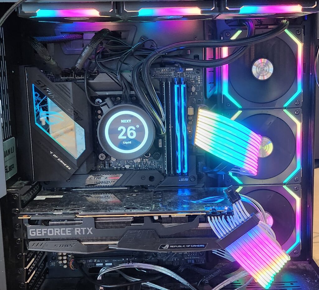
I set up a PC with 2×3 Lian Li Unifan SL 120 (top and side), 2 Lian Li Strimmer cables (an ATX and a PCIe), a NZXT Kraken Z73 CPU cooler (with LED screen, but cooled by the Lian Li Unifan SL 120 on the side, not the NZXT fans that came with it), 2 RGB DDR5 DRAMs, an ASUS ROG Geforce 2070 RTX Super, a Asus ROG Strix G690-F Gaming wifi and a Corsair K95 RGB Keyboard.
Happy rainbow colours! It seems to default to this every time I change stuff
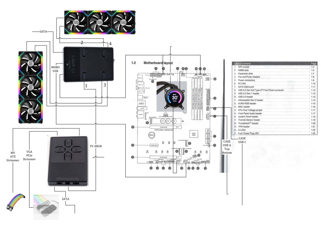
It’s no mean feat doing all the wiring on the fan controllers nowadays, and the instructions don’t make it much easier. Here is the wiring setup for this (excluding the keyboard)
The problem is that all of this hardware comes with it’s own bloated, janky software in order to get it to do stuff.
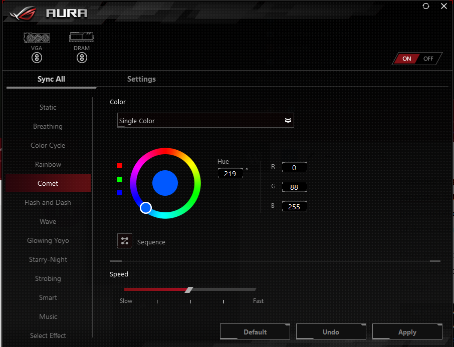
ASUS: Armory Crate / ASUS AURA
This thing takes up loads of memory and breaks often.
I decided to get rid of it once it had problems updating my drivers. You can still download Aura seperately (although there is a warning it will no longer be updated). To uninstall Armory Crate you can’t just uninstall everything from Add or Remove Programs, you need the uninstall tool, so it will also get rid of the scheduled tasks and a directory the windows uninstallers leave behind.
Once you install Aura seperately, it still takes an inane amount of processes, but you don’t actually need to run Aura to change the RGBs on the VGA and DRAM. Oddly enough not the motherboard itself though.
Just running AURA, not Armory Crate
You also can use other programs. Theoretically. That’s what the rest of this article is about. But in the end, I used Aura.
If you read on, it may be the case that I can’t get a lot of the other stuff to work because I don’t have Armory Crate installed. Nothing will work if I don’t have Aura installed, so I may as well use that.
Note: if you want to follow your driver updates, there’s a thread on the Republic of Gamers website that follows a whole load of them.
Problem I never solved: getting the Motherboard itself to show under Aura.
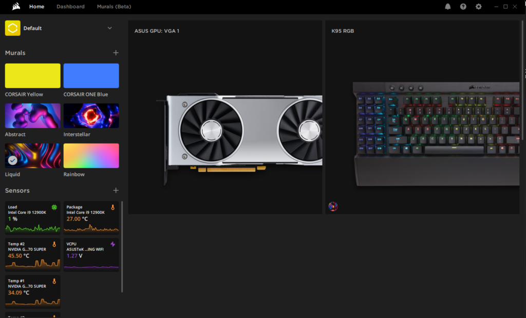
Corsiar: iCUE
Yup, this takes up memory, works pretty well, keeps updating for no apparent reason and I have to slide the switch left and right to get it to detect as a USB device quite often so the lighting works again. In terms of interface it’s quite easy to use.
Woohoo! all these processes for keyboard lighting!
It detects the motherboard and can monitor the motherboard, but can’t control the lighting on it. Once upon a time it did. Maybe this is because I’m not running the whole Armory Crate thing any more.
No idea.
Note: if you do put everything on in the dashboard, memory usage goes up to 500 MB
In fact, just having the iCUE screen open uses up ~200MB of memory.
It’s the most user friendly way of doing keyboard lighting effects though, so I keep it.
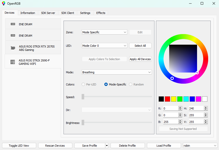
When I first started running it, it told me I needed to run it as an administrator to get a driver working. I ran it and it hung my computer at device detection. Later on it started rebooting it. After installing the underlying Asus Aura services running it ran for me. [Note: the following is for the standard 0.8 build: Once. It reboots my PC after device detection now. Lots of people on Reddit have it working, maybe it needs the Aura Crate software. I have opened an issue, hopefully it will get fixed? According to a Reddit user, this could be because “If you have armoury crate installed, OpenRGB cannot detect your motherboard, if your ram is ddr5 [note: which mine is], you’ll gonna have to wait or download the latest pipeline version”]
OK, so the Pipeline build does work and even detects my motherboard! Unfortunately it doesn’t write the setting to the motherboard, so after a reboot it goes back to rainbow. After my second attempt the setting seems to have stuck and survived the reboot. However it still hangs the computer on a reboot (everything turns off except the PC itself) and It can take quite some time to open the interface. It also sometimes does and sometimes doesn’t detect the DRAM modules. Issue opened here
Even with the interace open, the memory footprint is tiny!
Note that it saves the settings to C:\Users\razor\AppData\Roaming\OpenRGB an you can find the logs there too.
SignalRGB
This looks quite good at first glance – it detected my devices and was able to apply effects to all of them at once. Awesome! Unfortunately it has a huge memory footprint (around 600MB!) and doesn’t write the settings to the devices, so if after a reboot you don’t run SignalRGB the hardware won’t show any lighting at all, they will all be turned off.
It comes in a free tier with mostly anything you need and a paid subscription tier, which costs $4,- per month = $48,- per year! Considering what this does and the price of most of these kind of one trick pony utils (one time fee ~ $20) this is incredibly high. On Reddit the developers are aggressive in saying they need to keep developing in order to support new hardware and if you think they are charging a lot of money for this you are nuts. Also, in order to download the free effects you need an account with them.
So nope, not using this.
JackNet RGBSync
Another Open Source RGB software, I got it to detect my keyboard and not much else. Development has stopped in 2020. The UI leaves a lot to be desired.
Gigabyte RGB Fusion
Googling alternatives to Aura, you will run into this one. It’s not compatible with my rig and doesn’t detect anything. Not really too surprising, considering my stuff is all their competitor, Asus.
L-Connect 2 and 3
For the Lian Li fans and the Strimmer cables I use L-Connect 2. It has a setting saying it should take over the motherboard setting, but this has stopped working. Maybe I need Armory Crate. It’s a bit clunky (to change settings you need to select which fans in the array you want to send an effect to and it always shows 4 arrays of 4 fans, which I don’t actually have), but it writes settings to the devices so you don’t need it running in the background.
L-Connect 3 runs extremely slowly. It’s not hung, it’s just incredibly slow. Don’t know why, but could be Armory Crate related.
NZXT CAM
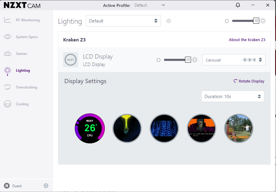
This you need in the background or the LED screen on the Kraken will show the default: CPU temperature only. It takes a very long time to start up. It also requires quite a bit of memory to run, which is pretty bizarre if all you want to do is show a few animated GIFs on your CPU cooler in carousel mode
Interface up on the screenRunning in the background
So, it’s shit but you really really need it if you want the display on the CPU cooler to work.
Fan Control
So not really RGB, but related, is Fan Control for Windows
Also G-helper works for fan control and gpu switching
Conclusion
None of the alternatives really works very well for me. None of them can control the Lian-Li strimmer devices and most of them only control a few of them or have prohibitive licenses attached for what they are. What is more, in order to use the alternatives, you still need to install the ASUS motherboard driver, which is exactly what I had been hoping to avoid. OpenRGB shows the most promise but is still not quite there yet – but it does work for a lot of people, so hopefully this will work for you too. Good luck and prepare to reboot… A lot!
[…] “With the help of a quantum annealer, we demonstrated a new way to pattern magnetic states,” said Alejandro Lopez-Bezanilla, a virtual experimentalist in the Theoretical Division at Los Alamos National Laboratory. Lopez-Bezanilla is the corresponding author of a paper about the research in Science Advances.
“We showed that a magnetic quasicrystal lattice can host states that go beyond the zero and one bit states of classical information technology,” Lopez-Bezanilla said. “By applying a magnetic field to a finite set of spins, we can morph the magnetic landscape of a quasicrystal object.”
[…]
Lopez-Bezanilla selected 201 qubits on the D-Wave computer and coupled them to each other to reproduce the shape of a Penrose quasicrystal.
Since Roger Penrose in the 1970s conceived the aperiodic structures named after him, no one had put a spin on each of their nodes to observe their behavior under the action of a magnetic field.
“I connected the qubits so all together they reproduced the geometry of one of his quasicrystals, the so-called P3,” Lopez-Bezanilla said. “To my surprise, I observed that applying specific external magnetic fields on the structure made some qubits exhibit both up and down orientations with the same probability, which leads the P3 quasicrystal to adopt a rich variety of magnetic shapes.”
Manipulating the interaction strength between qubits and the qubits with the external field causes the quasicrystals to settle into different magnetic arrangements, offering the prospect of encoding more than one bit of information in a single object.
Some of these configurations exhibit no precise ordering of the qubits’ orientation.
“This can play in our favor,” Lopez-Bezanilla said, “because they could potentially host a quantum quasiparticle of interest for information science.” A spin quasiparticle is able to carry information immune to external noise.
A quasiparticle is a convenient way to describe the collective behavior of a group of basic elements. Properties such as mass and charge can be ascribed to several spins moving as if they were one.
Upon first glance, the Unconventional Computing Laboratory looks like a regular workspace, with computers and scientific instruments lining its clean, smooth countertops. But if you look closely, the anomalies start appearing. A series of videos shared with PopSci show the weird quirks of this research: On top of the cluttered desks, there are large plastic containers with electrodes sticking out of a foam-like substance, and a massive motherboard with tiny oyster mushrooms growing on top of it.
[…]
Why? Integrating these complex dynamics and system architectures into computing infrastructure could in theory allow information to be processed and analyzed in new ways. And it’s definitely an idea that has gained ground recently, as seen through experimental biology-based algorithms and prototypes of microbe sensors and kombucha circuit boards.
In other words, they’re trying to see if mushrooms can carry out computing and sensing functions.
A mushroom motherboard. Andrew Adamatzky
With fungal computers, mycelium—the branching, web-like root structure of the fungus—acts as conductors as well as the electronic components of a computer. (Remember, mushrooms are only the fruiting body of the fungus.) They can receive and send electric signals, as well as retain memory.
“I mix mycelium cultures with hemp or with wood shavings, and then place it in closed plastic boxes and allow the mycelium to colonize the substrate, so everything then looks white,” says Andrew Adamatzky, director of the Unconventional Computing Laboratory at the University of the West of England in Bristol, UK. “Then we insert electrodes and record the electrical activity of the mycelium. So, through the stimulation, it becomes electrical activity, and then we get the response.” He notes that this is the UK’s only wet lab—one where chemical, liquid, or biological matter is present—in any department of computer science.
Preparing to record dynamics of electrical resistance of hemp shaving colonized by oyster fungi. Andrew Adamatzky
The classical computers today see problems as binaries: the ones and zeros that represent the traditional approach these devices use. However, most dynamics in the real world cannot always be captured through that system. This is the reason why researchers are working on technologies like quantum computers (which could better simulate molecules) and living brain cell-based chips (which could better mimic neural networks), because they can represent and process information in different ways, utilizing a series of complex, multi-dimensional functions, and provide more precise calculations for certain problems.
Already, scientists know that mushrooms stay connected with the environment and the organisms around them using a kind of “internet” communication. You may have heard this referred to as the wood wide web. By deciphering the language fungi use to send signals through this biological network, scientists might be able to not only get insights about the state of underground ecosystems, and also tap into them to improve our own information systems.
An illustration of the fruit bodies of Cordyceps fungi. Irina Petrova Adamatzky
Mushroom computers could offer some benefits over conventional computers. Although they can’t ever match the speeds of today’s modern machines, they could be more fault tolerant (they can self-regenerate), reconfigurable (they naturally grow and evolve), and consume very little energy.
Before stumbling upon mushrooms, Adamatzky worked on slime mold computers—yes, that involves using slime mold to carry out computing problems—from 2006 to 2016. Physarum, as slime molds are called scientifically, is an amoeba-like creature that spreads its mass amorphously across space.
Slime molds are “intelligent,” which means that they can figure out their way around problems, like finding the shortest path through a maze without programmers giving them exact instructions or parameters about what to do. Yet, they can be controlled as well through different types of stimuli, and be used to simulate logic gates, which are the basic building blocks for circuits and electronics.
Recording electrical potential spikes of hemp shaving colonized by oyster fungi. Andrew Adamatzky
Much of the work with slime molds was done on what are known as “Steiner tree” or “spanning tree” problems that are important in network design, and are solved by using pathfinding optimization algorithms. “With slime mold, we imitated pathways and roads. We even published a book on bio-evaluation of the road transport networks,” says Adamatzky “Also, we solved many problems with computation geometry. We also used slime molds to control robots.”
When he had wrapped up his slime mold projects, Adamatzky wondered if anything interesting would happen if they started working with mushrooms, an organism that’s both similar to, and wildly different from, Physarum. “We found actually that mushrooms produce action potential-like spikes. The same spikes as neurons produce,” he says. “We’re the first lab to report about spiking activity of fungi measured by microelectrodes, and the first to develop fungal computing and fungal electronics.”
An example of how spiking activity can be used to make gates. Andrew Adamatzky
In the brain, neurons use spiking activities and patterns to communicate signals, and this property has been mimicked to make artificial neural networks. Mycelium does something similar. That means researchers can use the presence or absence of a spike as their zero or one, and code the different timing and spacing of the spikes that are detected to correlate to the various gates seen in computer programming language (or, and, etc). Further, if you stimulate mycelium at two separate points, then conductivity between them increases, and they communicate faster, and more reliably, allowing memory to be established. This is like how brain cells form habits.
Mycelium with different geometries can compute different logical functions, and they can map these circuits based on the electrical responses they receive from it. “If you send electrons, they will spike,” says Adamatzky. “It’s possible to implement neuromorphic circuits… We can say I’m planning to make a brain from mushrooms.”
Hemp shavings in the shaping of a brain, injected with chemicals. Andrew Adamatzky
So far, they’ve worked with oyster fungi (Pleurotus djamor), ghost fungi (Omphalotus nidiformis), bracket fungi (Ganoderma resinaceum), Enoki fungi (Flammulina velutipes), split gill fungi (Schizophyllum commune) and caterpillar fungi (Cordyceps militari).
“Right now it’s just feasibility studies. We’re just demonstrating that it’s possible to implement computation, and it’s possible to implement basic logical circuits and basic electronic circuits with mycelium,” Adamatzky says. “In the future, we can grow more advanced mycelium computers and control devices.”
[…] In the latest advance in nano- and micro-architected materials, engineers at Caltech have developed a new material made from numerous interconnected microscale knots.
The knots make the material far tougher than identically structured but unknotted materials: they absorb more energy and are able to deform more while still being able to return to their original shape undamaged. These new knotted materials may find applications in biomedicine as well as in aerospace applications due to their durability, possible biocompatibility, and extreme deformability.
[…]
Each knot is around 70 micrometers in height and width, and each fiber has a radius of around 1.7 micrometers (around one-hundredth the radius of a human hair). While these are not the smallest knots ever made—in 2017 chemists tied a knot made from an individual strand of atoms—this does represent the first time that a material composed of numerous knots at this scale has ever been created. Further, it demonstrates the potential value of including these nanoscale knots in a material—for example, for suturing or tethering in biomedicine.
The knotted materials, which were created out of polymers, exhibit a tensile toughness that far surpasses materials that are unknotted but otherwise structurally identical, including ones where individual strands are interwoven instead of knotted. When compared to their unknotted counterparts, the knotted materials absorb 92 percent more energy and require more than twice the amount of strain to snap when pulled.
The knots were not tied but rather manufactured in a knotted state by using advanced high-resolution 3D lithography capable of producing structures in the nanoscale. The samples detailed in the Science Advancespaper contain simple knots—an overhand knot with an extra twist that provides additional friction to absorb additional energy while the material is stretched. In the future, the team plans to explore materials constructed from more complex knots.
[…]
More information: Widianto P. Moestopo et al, Knots are not for naught: Design, properties, and topology of hierarchical intertwined microarchitected materials, Science Advances (2023). DOI: 10.1126/sciadv.ade6725
[…] Human brains are slower than machines at processing simple information, such as arithmetic, but they far surpass machines in processing complex information as brains deal better with few and/or uncertain data. Brains can perform both sequential and parallel processing (whereas computers can do only the former), and they outperform computers in decision-making on large, highly heterogeneous, and incomplete datasets and other challenging forms of processing
[…]
fundamental differences between biological and machine learning in the mechanisms of implementation and their goals result in two drastically different efficiencies. First, biological learning uses far less power to solve computational problems. For example, a larval zebrafish navigates the world to successfully hunt prey and avoid predators (4) using only 0.1 microwatts (5), while a human adult consumes 100 watts, of which brain consumption constitutes 20% (6, 7). In contrast, clusters used to master state-of-the-art machine learning models typically operate at around 106 watts.
[…]
biological learning uses fewer observations to learn how to solve problems. For example, humans learn a simple “same-versus-different” task using around 10 training samples (12); simpler organisms, such as honeybees, also need remarkably few samples (~102) (13). In contrast, in 2011, machines could not learn these distinctions even with 106 samples (14) and in 2018, 107 samples remained insufficient (15). Thus, in this sense, at least, humans operate at a >106 times better data efficiency than modern machines
[…]
The power and efficiency advantages of biological computing over machine learning are multiplicative. If it takes the same amount of time per sample in a human or machine, then the total energy spent to learn a new task requires 1010 times more energy for the machine.
[…]
We have coined the term “organoid intelligence” (OI) to describe an emerging field aiming to expand the definition of biocomputing toward brain-directed OI computing, i.e. to leverage the self-assembled machinery of 3D human brain cell cultures (brain organoids) to memorize and compute inputs.
[…]
In this article, we present an architecture (Figure 1) and blueprint for an OI development and implementation program designed to:
● Determine the biofeedback characteristics of existing human brain organoids caged in microelectrode shells, potentially using AI to analyze recorded response patterns to electrical and chemical (neurotransmitters and their corresponding receptor agonists and antagonists) stimuli.
● Empirically test, refine, and, where needed, develop neurocomputational theories that elucidate the basis of in vivo biological intelligence and allow us to interact with and harness an OI system.
● Further scale up the brain organoid model to increase the quantity of biological matter, the complexity of brain organoids, the number of electrodes, algorithms for real-time interactions with brain organoids, and the connected input sources and output devices; and to develop big-data warehousing and machine learning methods to accommodate the resulting brain-directed computing capacity.
● Explore how this program could improve our understanding of the pathophysiology of neurodevelopmental and neurodegenerative disorders toward innovative approaches to treatment or prevention.
● Establish a community and a large-scale project to realize OI computing, taking full account of its ethical implications and developing a common ontology.
FIGURE 1
Figure 1 Architecture of an OI system for biological computing. At the core of OI is the 3D brain cell culture (organoid) that performs the computation. The learning potential of the organoid is optimized by culture conditions and enrichment by cells and genes critical for learning (including IEGs). The scalability, viability, and durability of the organoid are supported by integrated microfluidic systems. Various types of input can be provided to the organoid, including electrical and chemical signals, synthetic signals from machine sensors, and natural signals from connected sensory organoids (e.g. retinal). We anticipate high-resolution output measurement both by electrophysiological recordings obtained via specially designed 2D or 3D (shell) MEA, and potentially from implantable probes, and imaging of organoid structural and functional properties. These outputs can be used directly for computation purposes and as biofeedback to promote organoid learning. AI and machine learning are used throughout to encode and decode signals and to develop hybrid biocomputing solutions, in conjunction with a suitable big-data management system.
To the latter point, a community-forming workshop was held in February 2022 (51), which gave rise to the Baltimore Declaration Toward OI (52). It provides a statement of vision for an OI community that has led to the development of the program outlined here.
[…]
The past decade has seen a revolution in brain cell cultures, moving from traditional monolayer cultures to more organ-like, organized 3D cultures – i.e. brain organoids (Figure 2A). These can be generated either from embryonic stem cells or from the less ethically problematic iPSC typically derived from skin samples (54). The Johns Hopkins Center for Alternatives to Animal Testing, among others, has produced such brain organoids with high levels of standardization and scalability (32) (Figure 2B). Having a diameter below 500 μm, and comprising fewer than 100,000 cells, each organoid is roughly one 3-millionth the size of the human brain (theoretically equating to 800 MB of memory storage). Other groups have reported brain organoids with average diameters of 3–5 mm and prolonged culture times exceeding 1 year (34–36, 55–59).
FIGURE 2
Figure 2 Advances in 3D cell culturing provide the foundation for systems to explore organoid intelligence. (A) 3D neural cell cultures have important advantages for biological learning, compared with conventional 2D monolayers – namely a far greater density of cells, enhanced synaptogenesis, high levels of myelination, and enrichment by cell types essential to learning. (B) Brain organoid differentiation over time from 4 to 15 weeks, showing neurons (microtubule associated protein 2 [MAP2]; pink), oligodendrocytes (oligodendrocyte transcription factor [OLIG2]; red), and astrocytes (glial fibrillary acidic protein [GFAP]; green). Nuclei are stained with Hoechst 33342 (blue). Images were taken with an LCM 880 confocal microscope with 20x and 63x magnification. Scale bars are 100 μm and 20 μm, respectively. The images show the presence of MAP2-positive neurons as early as 4 weeks, while glial cells emerge at 8 weeks and there is a continuous increase in the number of astrocytes over time.
These organoids show various attributes that should improve their potential for biocomputing (Figure 2).
[…]
axons in these organoids show extensive myelination. Pamies et al. were the first to develop a 3D human brain model showing significant myelination of axons (32). About 40% of axons in the brain organoids were myelinated (30, 31), which approaches the 50% found in the human brain (60, 61). Myelination has since been reproduced in other brain organoids (47, 62). Myelin reduces the capacitance of the axonal membrane and enables saltatory conduction from one node of Ranvier to the next. As myelination increases electrical conductivity approximately 100-fold, this promises to boost biological computing performance, though its functional impact in this model remains to be demonstrated.
Finally, these organoid cultures can be enriched with various cell types involved in biological learning, namely oligodendrocytes, microglia, and astrocytes. Glia cells are integrally important for the pruning of synapses in biological learning (63–65) but have not yet been reported at physiologically relevant levels in brain organoid models. Preliminary work in our organoid model has shown the potential for astroglia cell expansion to physiologically relevant levels (47). Furthermore, recent evidence that oligodendrocytes and astrocytes significantly contribute to learning plasticity and memory suggests that these processes should be studied from a neuron-to-glia perspective, rather than the neuron-to-neuron paradigm generally used (63–65). In addition, optimizing the cell culture conditions to allow the expression of immediate early genes (IEGs) is expected to further boost the learning and memory capacities of brain organoids since these are key to learning processes and are expressed only in neurons involved in memory formation
AMD’s client PC sales also dropped dramatically—a whopping 51 percent year-over-year—but the company managed to eke out a small profit despite the sky falling. So why aren’t CPU and GPU prices falling too? In a call with investors Tuesday night, CEO Lisa Su confirmed that AMD has been “undershipping” chips for a while now to balance supply and demand (read: keep prices up).
“We have been undershipping the sell-through or consumption for the last two quarters,” Su said, as spotted by PC Gamer. “We undershipped in Q3, we undershipped in Q4. We will undership, to a lesser extent, in Q1.”
With the pandemic winding down and inflation ramping up, far fewer people are buying CPUs, GPUs, and PCs. It’s a hard, sudden reverse from just months ago, when companies like Nvidia and AMD were churning out graphic cards as quickly as possible to keep up with booming demand from cryptocurrency miners and PC gamers alike. Now that GPU mining is dead, shelves are brimming with unsold chips.
Despite the painfully high price tags of new next-gen GPUs, last-gen GeForce RTX 30-series and Radeon RX 6000-series graphics cards are still selling for very high prices considering their two-year-old status. Strategic under-shipping helps companies maintain higher prices for their wares.
[…]
AMD isn’t the only one doing it, either.
“We’re continuing to watch each and every day in terms of the sell-through that we’re seeing,” Nvidia CFO Colette Kress said to investors in November. “So we have been undershipping. We have been undershipping gaming at this time so that we can correct that inventory that is out in the channel.”
Since then, Nvidia has released the $1,200 GeForce RTX 4080 and $800 RTX 4070 Ti, two wildly overpriced graphics cards, and tried positioning them as enthusiast-grade upsells over the RTX 30-series, rather than treating them like the usual cyclical upgrades. AMD’s $900 Radeon RX 7900 XT offers similarly disappointing value and the company recently released a blog post also positioning its new GPUs as enthusiast-grade upsells.
[…]
We expect—hope?—that as stocks dwindle down and competition ramps up, sanity will return to graphics card prices, mirroring AMD and Intel’s recent CPU price adjustments. Just this morning, Intel announced that its Arc A750 graphics card was getting a price cut to $250, instantly making it an all-too-rare tempting target for PC gamers on a budget.
Secondhand MacBooks that retailed for as much as $3,000 are being turned into parts because recyclers have no way to login and factory reset the machines, which are often just a couple years old.
“How many of you out there would like a 2-year-old M1 MacBook? Well, too bad, because your local recycler just took out all the Activation Locked logic boards and ground them into carcinogenic dust,” John Bumstead, a MacBook refurbisher and owner of the RDKL INC repair store, said in a recent tweet.
The problem is Apple’s T2 security chip. First introduced in 2018, the laptop makes it impossible for anyone who isn’t the original owner to log into the machine. It’s a boon for security and privacy and a plague on the second hard market. “Like it has been for years with recyclers and millions of iPhones and iPads, it’s pretty much game over with MacBooks now—there’s just nothing to do about it if a device is locked,” Bumstead told Motherboard. “Even the jailbreakers/bypassers don’t have a solution, and they probably won’t because Apple proprietary chips are so relatively formidable.” When Apple released its own silicon with the M1, it integrated the features of the T2 into those computers.
[…]
Bumstead told Motherboard that every year Apple makes life a little harder for the second hand market. “The progression has been, first you had certifications with unrealistic data destruction requirements, and that caused recyclers to pull drives from machines and sell without drives, but then as of 2016 the drives were embedded in the boards, so they started pulling boards instead,” he said. “And now the boards are locked, so they are essentially worthless. You can’t even boot locked 2018+ MacBooks to an external device because by default the MacBook security app disables external booting.”
Motherboard first reported on this problem in 2020, but Bumstead said it’s gotten worse recently. “Now we’re seeing quantity come through because companies with internal 3-year product cycles are starting to dump their 2018/2019s, and inevitably a lot of those are locked,” he said.
[…]
Bumstead offered some solutions to the problem. “When we come upon a locked machine that was legally acquired, we should be able to log into our Apple account, enter the serial and any given information, then click a button and submit the machine to Apple for unlocking,” he said. “Then Apple could explore its records, query the original owner if it wants, but then at the end of the day if there are no red flags and the original owner does not protest within 30 days, the device should be auto-unlocked.”
In what looks like a victory for farmers in the United States, the American Farm Bureau Federation (AFBF) has struck a Memorandum of Understanding (MoU) with equipment vendor John Deere regarding the repairability of its machines.
As farming has become more technology-driven, Deere has increasingly injected software into its products with all of its tractors and harvesters now including an autopilot feature as standard.
There is also the John Deere Operations Center, which “instantly captures vital operational data to boost transparency and increase productivity for your business.”
Within a matter of years, the company envisages having 1.5 million machines and half a billion acres of land connected to the cloud service, which will “collect and store crop data, including millions of images of weeds that can be targeted by herbicide.”
Deere also estimates that software fees will make up 10 percent of the company’s revenues by the end of the decade, with Bernstein analysts pegging the average gross margin for farming software at 85 percent, compared to 25 percent for equipment sales.
Just like other commercial software vendors, however, Deere exercises close control and restricts what can be done with its products. This led farm labor advocacy groups to file a complaint to the US Federal Trade Commission last year, claiming that Deere unlawfully refused to provide the software and technical data necessary to repair its machinery.
“Deere is the dominant force in the $68 billion US agricultural equipment market, controlling over 50 per cent of the market for large tractors and combines,” said Fairmark Partners, the groups’ attorneys, in a preface to the complaint [PDF].
“For many farmers and ranchers, they effectively have no choice but to purchase their equipment from Deere. Not satisfied with dominating just the market for equipment, Deere has sought to leverage its power in that market to monopolize the market for repairs of that equipment, to the detriment of farmers, ranchers, and independent repair providers.”
[…]
The MoU, which can be read here [PDF], was signed yesterday at the 2023 AFBF Convention in San Juan, Puerto Rico, and seems to be a commitment by Deere to improve farmers’ access and choice when it comes to repairs.
[…]
Duvall said on a podcast about the matter that the MoU is the result of several years’ work. “As you use equipment, we all know at some point in time, there’s going to be problems with it. And we did have problems with having the opportunity to repair our equipment where we wanted to, or even repair it on the farm,” he added.
“It ensures that our farmers can repair their equipment and have access to the diagnostic tools and product guides so that they can find the problems and find solutions for them. And this is the beginning of a process that we think is going to be real healthy for our farmers and for the company because what it does is it sets up an opportunity for our farmers to really work with John Deere on a personal basis.”
Mercedes raised some worried eyebrows with its recent announcement to offer additional power for its EVs via subscription. For electric EQE and EQS models, Mercedes will bump their horsepower if customers pay an additional $1,200 per year. However, that’s going to remain a U.S. market service only for the time being, as Europe currently won’t allow Mercedes to offer it, according to this report from Top Gear NL.
A spokesperson for Mercedes Netherlands told Top Gear NL that legal matters currently prevent Mercedes from offering a subscription-based power upgrade. However, the spokesperson declined to comment further, so it’s currently unknown what sort of laws block such subscription-based services. Especially when there are other subscription services that are available in Europe, such as BMW’s heated seat subscription. Automakers can also update a car’s horsepower, via free over-the-air service updates, as both Polestar and Tesla do so in Europe. But that comes at no extra cost and is a one-time, permanent upgrade. So there seems to be some sort of legal issue with charging a yearly subscription for horsepower.
In the U.S. market, Mercedes’ $1,200 yearly subscription gets EQE and EQS owners nearly a 100 horsepower gain. However, because it’s only software that unlocks the power, it’s obvious that the powertrain is capable of that much power regardless of subscription. So customers might feel cheated that they’re paying for a car with a powertrain that’s intentionally hamstrung from the factory, with its full potential hidden behind a paywall.
Let’s hope that this gets regulated properly at EU level – it’s bizarre that you can’t use something you paid for because it’s disabled and can be re-enabled remotely.
Intel and AMD did something like this in 2010 in a process called binning where they artificially disabled features in the hardware:
As Engadget rather calmly points out, Intel has been testing the waters with a new “Upgrade Card” system, which essentially involves buying a $50 scratch card with a code that unlocks features in your PC’s processor.
The guys at Hardware.info broke this story last month, although nobody seemed to notice right away—perhaps because their site’s in Dutch. The article shows how the upgrade key unlocks “an extra megabyte L3 cache and Hyper Threading” on the Pentium G6951. In its locked state, that 2.8GHz processor has two physical cores, two threads, and 3MB of L3 cache, just like the retail-boxed Pentium G6950.
[…]
Detractors of the scheme might point out that Intel is making customers pay for features already present in the CPU they purchased. That’s quite true. However, as the Engadget post notes, both Intel and AMD have been selling CPUs with bits and pieces artificially disabled for years. That practice is known as binning—sometimes, chipmakers use it to unload parts with malfunctioning components; other times, it’s more about product segmentation and demand. There have often been unofficial workarounds, too. These days, for example, quite a few AMD motherboards let you unlock cores in Athlon II X3 and Phenom II X2 processors. Intel simply seems to be offering an official workaround for its CPUs… and cashing in on it.
As the cryptocurrency market currently goes through one of its worst nosedives in recent years, miners are trying to get rid of their mining hardware. Due to the crashing prices of popular crypto coins, numerous Chinese miners and e-cafes are flooding the market with graphics cards they no longer need.
Miners, e-cafes, and scalpers are now trying to sell their hardware stock on streams and auctions. As a result, users can snag a second-hand GPU, such as the RTX 3060 Ti, for $350 or even less. Many popular graphics cards going for MSRP or even less is quite a sight to behold after astronomically high prices and scarce availability during the last two years.
GPU flood is here.
Chinese miners and South Asian ecafes now dismantling their mining rigs and putting cards up for auction on livestreams.
As tempting as it might be to snag a powerful Nvidia or AMD GPU for a price lower than its MSRP, it is not the best idea to go after a graphics card that went through seven rings of mining hell. Potential buyers should be aware that the mining GPUs are often not in their best conditions after spending months in always-on, always-100% mode.
With manufacturers increasing their supply and prices going down like never before, you may better spend a little more and get a new graphics card with a warranty and peace of mind. As a bonus, you can enjoy the view of scalpers getting desperate to get at least some money from their stock.
Last year, researchers from the National Taiwan University’s Interactive Graphics (and Multimedia) Laboratory and the National Chengchi University revealed their Hair Touch controller at the 2021 Computer-Human Interaction conference. The bizarre-looking contraption featured a tuft of hair that could be extended and contracted so that when someone tried to pet a virtual cat, or interact with other furry objects in virtual reality, their fingers would actually feel the fur, as far as their brains were concerned.
That was more or less the same motivation for researchers from the Korea Advanced Institute of Science and Technology’s MAKinteract Lab to create the SpinOcchio VR controller. Instead of making virtual fur feel real, the controller is designed to recreate the feeling of slipping something between your fingers. In the researchers’ own words, it’s described as “a handheld haptic controller capable of rendering the thickness and slipping of a virtual object pinched between two fingers.”
To keep this story PG-13, let’s stick with one of the example use cases the researchers suggest for the SpinOcchio controller: virtual pottery. Making bowls, vases, and other ceramics on a potter’s wheel in real life requires the artist to be able to feel the spinning object in their hands in order to make it perfectly cylindrical and stable. Attempting to use a potter’s wheel in virtual reality with a pair of VR joysticks in hand is nowhere near the same experience, but that’s the ultimate goal of VR: to accurately recreate an experience that otherwise may be inaccessible to a user.
Scientists from the Physics and Engineering Department of the UK’s Lancaster University have published a paper detailing a breakthrough in the mass production of UltraRAM. Researchers have pondered over this novel memory type for several years due to its highly attractive qualities, and the latest breakthrough means that mass production on silicon wafers could be within sight. UltraRAM is described as a memory technology which “combines the non-volatility of a data storage memory, like flash, with the speed, energy-efficiency, and endurance of a working memory, like DRAM.”
(Image credit: Lancaster University)
Importantly, UltraRAM on silicon could be the universal memory type that will one day cater to all the memory needs (both RAM and storage) of PCs and devices.
[…]
The fundamental science behind UltraRAM is that it uses the unique properties of compound semiconductors, commonly used in photonic devices such as LEDs, lasers, and infrared detectors can now be mass-produced on silicon. The researchers claim that the latest incarnation on silicon outperforms the technology as tested on Gallium Arsenide semiconductor wafers.
(Image credit: Lancaster University)
Some extrapolated numbers for UltraRAM are that it will offer “data storage times of at least 1,000 years,” and its fast switching speed and program-erase cycling endurance is “one hundred to one thousand times better than flash.” Add these qualities to the DRAM-like speed, energy efficiency, and endurance, and this novel memory type sounds hard for tech companies to ignore.
If you read between the lines above, you can see that UltraRAM is envisioned to break the divide between RAM and storage. So, in theory, you could use it as a one-shot solution to fill these currently separate requirements. In a PC system, that would mean you would get a chunk of UltraRAM, say 2TB, and that would cover both your RAM and storage needs.
The shift, if it lives up to its potential, would be a great way to push forward with the popular trend towards in-memory processing. After all, your storage would be your memory – with UltraRAM; it is the same silicon.