Sonos CEO apologizes for confusion, says legacy products will work ‘as long as possible’ – however long that is

Sonos CEO Patrick Spence just published a statement on the company’s website to try to clear up an announcement made earlier this week: on Tuesday, Sonos announced that it will cease delivering software updates and new features to its oldest products in May. The company said those devices should continue functioning properly in the near term, but it wasn’t enough to prevent an uproar from longtime customers, with many blasting Sonos for what they perceive as planned obsolescence. That frustration is what Spence is responding to today. “We heard you,” is how Spence begins the letter to customers. “We did not get this right from the start.”

Spence apologizes for any confusion and reiterates that the so-called legacy products will “continue to work as they do today.” Legacy products include the original Sonos Play:5, Zone Players, and Connect / Connect:Amp devices manufactured between 2011 and 2015.

“Many of you have invested heavily in your Sonos systems, and we intend to honor that investment for as long as possible.” Similarly, Spence pledges that Sonos will deliver bug fixes and security patches to legacy products “for as long as possible” — without any hard timeline. Most interesting, he says “if we run into something core to the experience that can’t be addressed, we’ll work to offer an alternative solution and let you know about any changes you’ll see in your experience.”

The letter from Sonos’ CEO doesn’t retract anything that the company announced earlier this week; Spence is just trying to be as clear as possible about what’s happening come May. Sonos has insisted that these products, some of which are a decade old, have been taken to their technological limits.

Spence again confirms that Sonos is planning a way for customers to fork any legacy devices they might own off of their main Sonos system with more modern speakers. (Sonos architected its system so that all devices share the same software. Once one product is no longer eligible for updates, the whole setup stops receiving them. This workaround is designed to avoid that problem.)

Source: Sonos CEO apologizes for confusion, says legacy products will work ‘as long as possible’ – The Verge

An Open Source eReader That’s Free of Corporate Restrictions Is Exactly What I Want Right Now

The Open Book Project was born from a contest held by Hackaday and that encouraged hardware hackers to find innovative and practical uses for the Arduino-based Adafruit Feather development board ecosystem. The winner of that contest was the Open Book Project which has been designed and engineered from the ground up to be everything devices like the Amazon Kindle or Rakuten Kobo are not. There are no secrets inside the Open Book, no hidden chips designed to track and share your reading habits and preferences with a faceless corporation. With enough know-how, you could theoretically build and program your own Open Book from scratch, but as a result of winning the Take Flight With Feather contest, Digi-Key will be producing a small manufacturing run of the ereader, with pricing and availability still to be revealed.

The raw hardware isn’t as sleek or pretty as devices like the Kindle, but at the same time there’s a certain appeal to the exposed circuit board which features brief descriptions of various components, ports, and connections etched right onto the board itself for those looking to tinker or upgrade the hardware. Users are encouraged to design their own enclosures for the Open Book if they prefer, either through 3D-printed cases made of plastic, or rustic wooden enclosures created using laser cutting machines.

Text will look a little aliased on the Open Book’s E Ink display.
Photo: Hackaday.io

With a resolution of just 400×300 pixels on its monochromatic E Ink display, text on the Open Book won’t look as pretty as it does on the Amazon Kindle Oasis which boasts a resolution of 1,680×1,264 pixels, but it should barely sip power from its built-in lithium-polymer rechargeable battery—a key benefit of using electronic paper.

The open source ereader—powered by an ARM Cortex M4 processor—will also include a headphone jack for listening to audio books, a dedicated flash chip for storing language files with specific character sets, and even a microphone that leverages a TensorFlow-trained AI model to intelligently process voice commands so you can quietly mutter “next!” to turn the page instead of reaching for one of the ereader’s physical buttons like a neanderthal. It can also be upgraded with additional functionality such as Bluetooth or wifi using Adafruit Feather expansion boards, but the most important feature is simply a microSD card slot allowing users to load whatever electronic text and ebook files they want. They won’t have to be limited by what a giant corporation approves for its online book store, or be subject to price-fixing schemes which, for some reason, have still resulted in electronic files costing more than printed books.

What remains to be seen is whether or not the Open Book Project can deliver an ereader that’s significantly cheaper than what Amazon or Rakuten has delivered to consumers. Both of those companies benefit from the economy of scale having sold millions of devices to date, and are able to throw their weight around when it comes to manufacturing costs and sourcing hardware. If the Open Book can be churned out for less than $50, it could potentially provide some solid competition to the limited ereader options currently out there.

Source: An Open Source eReader That’s Free of Corporate Restrictions Is Exactly What I Want Right Now

Apple’s latest AI acquisition leaves some Wyze cameras without people detection

Earlier today, Apple confirmed it purchased Seattle-based AI company Xnor.ai (via MacRumors). Acquisitions at Apple’s scale happen frequently, though rarely do they impact everyday people on the day of their announcement. This one is different.

Cameras from fellow Seattle-based company Wyze, including the Wyze Cam V2 and Wyze Cam Pan, have utilized Xnor.ai’s on-device people detection since last summer. But now that Apple owns the company, it’s no longer available. Some people on Wyze’s forum are noting that the beta firmware removing the people detection has already started to roll out.

Oddly enough, word of this lapse in service isn’t anything new. Wyze issued a statement in November 2019 saying that Xnor.ai had terminated their contract (though its reason for doing so wasn’t as clear then as it is today), and that a firmware update slated for mid-January 2020 would remove the feature from those cameras.

There’s a bright side to this loss, though, even if Apple snapping up Xnor.ai makes Wyze’s affordable cameras less appealing in the interim. Wyze says that it’s working on its own in-house version of people detection for launch at some point this year. And whether it operates on-device via “edge AI” computing like Xnor.ai’s does, or by authenticating through the cloud, it will be free for users when it launches.

That’s good and all, but the year just started, and it’s a little worrying Wyze hasn’t followed up with a specific time frame for its replacement of the feature. Two days ago, Wyze’s social media community manager stated that the company was “making great progress” on its forums, but they didn’t offer up when it would be available.

As for what Apple plans to do with Xnor.ai is anyone’s guess. Ahead of its partnership with Wyze, the AI startup had developed a small, wireless AI camera that ran exclusively on solar power. Regardless of whether Apple is more interested in its edge computing algorithm, as was seen working on Wyze cameras for a short time, or its clever hardware ideas around AI-powered cameras, it’s getting all of it with the purchase.

Source: Apple’s latest AI acquisition leaves some Wyze cameras without people detection – The Verge

Amazon, Apple, Google, and the Zigbee Alliance joined together to form working group to develop open standard for smart home devices

Amazon, Apple, Google, and the Zigbee Alliance joined together to promote the formation of the Working Group. Zigbee Alliance board member companies IKEA, Legrand, NXP Semiconductors, Resideo, Samsung SmartThings, Schneider Electric, Signify (formerly Philips Lighting), Silicon Labs, Somfy, and Wulian are also on board to join the Working Group and contribute to the project.

The goal of the Connected Home over IP project is to simplify development for manufacturers and increase compatibility for consumers. The project is built around a shared belief that smart home devices should be secure, reliable, and seamless to use. By building upon Internet Protocol (IP), the project aims to enable communication across smart home devices, mobile apps, and cloud services and to define a specific set of IP-based networking technologies for device certification.

The industry Working Group will take an open-source approach for the development and implementation of a new, unified connectivity protocol. The project intends to use contributions from market-tested smart home technologies from Amazon, Apple, Google, Zigbee Alliance, and others. The decision to leverage these technologies is expected to accelerate the development of the protocol, and deliver benefits to manufacturers and consumers faster.

The project aims to make it easier for device manufacturers to build devices that are compatible with smart home and voice services such as Amazon’s Alexa, Apple’s Siri, Google’s Assistant, and others. The planned protocol will complement existing technologies, and Working Group members encourage device manufacturers to continue innovating using technologies available today.

Source: Project Connected Home over IP

Getting Drivers for Old Hardware Is Harder Than Ever

despite the fact that all the drivers generally have to do is simply sit on the internet, available when they’re necessary.

Apparently, that isn’t easy enough for Intel. Recently, the chipmaker took BIOS drivers, a boot-level firmware technology used for hardware initialization in earlier generations of PCs, for a number of its unsupported motherboards off its website, citing the fact that the programs have reached an “End of Life” status. While it reflects the fact that Unified Extensible Firmware Interface (UEFI), a later generation of firmware technology used in PCs and Macs, is expected to ultimately replace BIOS entirely, it also leaves lots of users with old gadgets out in a lurch. And as Bleeping Computer has noted, it appears to be part of a broader trend to prevent downloads for unsupported hardware on the Intel website—things that have long lived past their current lives. After all, if something goes wrong, Intel can be sure it’s not liable if a 15-year-old BIOS update borks a system.

In a comment to Motherboard, Intel characterized the approach to and timing of the removals as reflecting industry norms.

[…]

However, this is a problem for folks who take collecting or use of old technology seriously, such as those on the forum Vogons, which noticed the issue first, though it’s far from anything new. Technology companies come and go all the time, and as things like mergers and redesigns happen, often the software repository gets affected when the technology goes out of date.

A Problem For Consumers & Collectors

Jason Scott, the Internet Archive’s lead software curator, says that Intel’s decision to no longer provide old drivers on its website reflects a tendency by hardware and software developers to ignore their legacies when possible—particularly in the case of consumer software, rather than in the enterprise, where companies’ willingness to pay for updates ensures that needed updates won’t simply sit on the shelf.

[…]

By the mid-90s, companies started to create FTP repositories to distribute software, which had the effect of changing the nature of updates: When the internet made distribution easier and both innovation and security risks grew more advanced, technology companies updated their apps far more often.

FTP’s Pending Fadeout

Many of those FTP servers are still around today, but the news cycle offers a separate, equally disappointing piece of information for those looking for vintage drivers: Major web browsers are planning to sunset support for the FTP protocol. Chrome plans to remove support for FTP sites by version 82, which is currently in the development cycle and will hit sometime next year. And Firefox makers Mozilla have made rumblings about doing the same thing.

The reasons for doing so, often cited for similar removals of legacy features, come down to security. FTP is a legacy service that can’t be secured in much the same way that its successor, SFTP, can.

While FTP applications like CyberDuck will likely exist for decades from now, the disconnect from the web browser will make these servers a lot harder to use. The reason goes back to the fact that the FTP protocol isn’t inherently searchable—but the best way to find information about it is with a web-based search engine … such as Google.

[…]

Earlier this year, I was attempting to get a vintage webcam working, and while I was ultimately unable to get it to work, it wasn’t due to lack of software access. See, Logitech actually kept copies of Connectix’s old webcam software on its FTP site. This is software that hasn’t seen updates in more than 20 years; that only supports Windows 3.1, Windows NT, and Windows 95; and that wasn’t on Logitech’s website.

One has to wonder how soon those links will disappear from Google searches once the two most popular desktop browsers remove easy access to those files. And there’s no guarantee that a company is going to keep a server online beyond that point.

“It was just it was this weird experience that FTP sites, especially, could have an inertia of 15 to 20 years now, where they could be running all this time, untouched,” Scott added. “And just every time that, you know, if the machine dies, it goes away.”

Source: Getting Drivers for Old Hardware Is Harder Than Ever – VICE

Nikon Is Killing Its Authorized Repair Program

Nikon is ending its authorized repair program in early 2020, likely leaving more than a dozen repair shops without access to official parts and tools, and cutting the number of places you can get your camera fixed with official parts from more than a dozen independent shops to two facilities at the ends of the U.S.

That means that Nikon’s roughly 15 remaining Authorized Repair Station members are about to become non-authorized repair shops. Since Nikon decided to stop selling genuine parts to non-authorized shops back in 2012, it’s unlikely those stores will continue to have access to the specialty components, tools, software, manuals, and model training Nikon previously provided. But Nikon hasn’t clarified this, so repair shops have been left in the dark.

“This is very big, and we have no idea what’s coming next,” said Cliff Hanks, parts manager for Kurt’s Camera Repair in San Diego, Calif. “We need more information before March 31. We can make contingency plans, start stocking up on stuff, but when will we know for sure?”

In a letter obtained by iFixit, Nikon USA told its roughly 15 remaining Authorized Repair Station members in early November that it would not renew their agreements after March 31, 2020. The letter notes that “The climate in which we do business has evolved, and Nikon Inc. must do the same.” And so, Nikon writes, it must “change the manner in which we make product service available to our end user customers.”

In other words: Nikon’s camera business, slowly bled by smartphones, is going to adopt a repair model that’s even more restrictive than that of Apple or other smartphone makers. If your camera breaks, and you want it fixed with official parts or under warranty, you’ll now have to mail it to one of two ends of the country. This is more than a little inconvenient, especially for professional photographers.

Source: Nikon Is Killing Its Authorized Repair Program – iFixit

System76 Will Begin Shipping 2 Linux Laptops With Coreboot-Based Open Source Firmware

System76, the Denver-based Linux PC manufacturer and developer of Pop OS, has some stellar news for those of us who prefer our laptops a little more open. Later this month the company will begin shipping two of their laptop models with its Coreboot-powered open source firmware.

Beginning today, System76 will start taking pre-orders for both the Galago Pro and Darter Pro laptops. The systems will ship out later in October, and include the company’s Coreboot-based open source firmware which was previously teased at the 2019 Open Source Firmware Conference.

(Coreboot, formerly known as LinuxBIOS, is a software project aimed at replacing proprietary firmware found in most computers with a lightweight firmware designed to perform only the minimum number of tasks necessary to load and run a modern 32-bit or 64-bit operating system.)

What’s so great about ripping out the proprietary firmware included in machines like this and replacing it with an open alternative? To begin with, it’s leaner. System76 claims that users can boot from power off to the desktop 29% faster with its Coreboot-based firmware.

Source: System76 Will Begin Shipping 2 Linux Laptops With Coreboot-Based Open Source Firmware

MIT Researchers Build Functional Carbon Nanotube Microprocessor

Scientists at MIT built a 16-bit microprocessor out of carbon nanotubes and even ran a program on it, a new paper reports.

Silicon-based computer processors seem to be approaching a limit to how small they can be scaled, so researchers are looking for other materials that might make for useful processors. It appears that transistors made from tubes of rolled-up, single-atom-thick sheets of carbon, called carbon nanotubes, could one day have more computational power while requiring less energy than silicon.

[…]

the MIT group, led by Gage Hills and Christian Lau, has now debuted a functional 16-bit processor called RV16X-NANO that uses carbon nanotubes, rather than silicon, for its transistors. The processor was constructed using the same industry-standard processes behind silicon chips—Shulaker explained that it’s basically just a silicon microprocessor with carbon nanotubes instead of silicon.

The processor works well enough to run HELLO WORLD, a program that simply outputs the phrase “HELLO WORLD” and is the first program that most coding students learn. Shulaker compared its performance to a processor you’d buy at hobby shop to control a small robot.

[…]

A small but notable fraction of carbon nanotubes act like conductors instead of semiconductors. Shulaker explained that study author Hills devised a technique called DREAM, where the circuits were specifically designed to work despite the presence of metallic nanotubes. And of course, the effort relied on the contribution of every member of the relatively small team. The researchers published their results in the journal Nature today.

[…]

Ultimately, the goal isn’t to erase the decades of progress made by silicon microchips—perhaps companies can integrate carbon nanotube pieces into existing architectures.

This is still a proof-of-concept. The team still hasn’t calculated the chip’s performance or whether it’s actually more energy efficient than silicon—the gains are based on projections. But Shulaker hopes that the team’s work will serve as a roadmap toward incorporating carbon nanotubes in computers for the future.

Source: MIT Researchers Build Functional Carbon Nanotube Microprocessor

Researchers build a heat shield just 10 atoms thick to protect electronic devices

Excess heat given off by smartphones, laptops and other electronic devices can be annoying, but beyond that it contributes to malfunctions and, in extreme cases, can even cause lithium batteries to explode.

To guard against such ills, engineers often insert glass, plastic or even layers of air as insulation to prevent heat-generating components like microprocessors from causing damage or discomforting users.

Now, Stanford researchers have shown that a few layers of atomically , stacked like sheets of paper atop hot spots, can provide the same insulation as a sheet of glass 100 times thicker. In the near term, thinner heat shields will enable engineers to make even more compact than those we have today, said Eric Pop, professor of electrical engineering and senior author of a paper published Aug. 16 in Science Advances.

[…]

To make nanoscale heat shields practical, the researchers will have to find some mass production technique to spray or otherwise deposit atom-thin layers of materials onto electronic components during manufacturing. But behind the immediate goal of developing thinner insulators looms a larger ambition: Scientists hope to one day control the vibrational energy inside materials the way they now control electricity and light. As they come to understand the heat in solid objects as a form of sound, a new field of phononics is emerging, a name taken from the Greek root word behind telephone, phonograph and phonetics.

“As engineers, we know quite a lot about how to control electricity, and we’re getting better with light, but we’re just starting to understand how to manipulate the high-frequency sound that manifests itself as at the atomic scale,” Pop said.

Source: Researchers build a heat shield just 10 atoms thick to protect electronic devices

Apple Is Locking iPhone Batteries to Discourage Repair, showing ominous errors if you replace your battery

By activating a dormant software lock on their newest iPhones, Apple is effectively announcing a drastic new policy: only Apple batteries can go in iPhones, and only they can install them.

If you replace the battery in the newest iPhones, a message indicating you need to service your battery appears in Settings > Battery, next to Battery Health. The “Service” message is normally an indication that the battery is degraded and needs to be replaced. The message still shows up when you put in a brand new battery, however. Here’s the bigger problem: our lab tests confirmed that even when you swap in a genuine Apple battery, the phone will still display the “Service” message.

It’s not a bug; it’s a feature Apple wants. Unless an Apple Genius or an Apple Authorized Service Provider authenticates a battery to the phone, that phone will never show its battery health and always report a vague, ominous problem.

Source: Apple Is Locking iPhone Batteries to Discourage Repair – iFixit

Quantum interference allows huge data sets to be sifted through much more quickly

Contemporary science, medicine, engineering and information technology demand efficient processing of data—still images, sound and radio signals, as well as information coming from different sensors and cameras. Since the 1970s, this has been achieved by means of the Fast Fourier Transform algorithm (FFT). The FFT makes it possible to efficiently compress and transmit data, store pictures, broadcast digital TV, and talk over a mobile phone. Without this algorithm, medical imaging systems based on magnetic resonance or ultrasound would not have been developed. However, it is still too slow for many demanding applications.

To meet this goal, scientists have been trying for years to harness quantum mechanics. This resulted in the development of a quantum counterpart of the FFT, the Quantum Fourier Transform (QFT), which can be realized with a quantum computer. As the quantum computer simultaneously processes all possible values (so-called “superpositions”) of input data, the number of operations decreases considerably.

[…]

Mathematics describes many transforms. One of them is a Kravchuk transform. It is very similar to the FFT, as it allows processing of discrete (e.g. digital) data, but uses Kravchuk functions to decompose the input sequence into the spectrum. At the end of the 1990s, the Kravchuk transform was “rediscovered” in computer science. It turned out to be excellent for image and sound processing. It allowed scientists to develop new and much more precise algorithms for the recognition of printed and handwritten text (including even the Chinese language), gestures, sign language, people, and faces. A dozen years ago, it was shown that this transform is ideal for processing low-quality, noisy and distorted data, and thus it could be used for computer vision in robotics and autonomous vehicles. There is no fast algorithm to compute this transform, but it turns out that quantum mechanics allows one to circumvent this limitation.

“Holy Grail” of computer science

In their article published in Science Advances, scientists from the University of Warsaw—Dr. Magdalena Stobinska and Dr. Adam Buraczewski, scientists from the University of Oxford, and NIST, have shown that the simplest quantum gate, which interferes between two quantum states, essentially computes the Kravchuk transform. Such a gate could be a well-known optical device—a beam splitter, which divides photons between two outputs. When two states of quantum light enter its input ports from two sides, they interfere. For example, two identical photons, which simultaneously enter this device, bunch into pairs and come out together by the same exit port. This is the well-known Hong-Ou-Mandel effect, which can also be extended to states made of many particles. By interfering “packets” consisting of many indistinguishable photons (indistinguishability is very important, as its absence destroys the quantum effect), which encode the information, one obtains a specialized quantum computer that computes the Kravchuk transform.

The experiment was performed in a quantum optical laboratory at the Department of Physics at the University of Oxford, where a special setup was built to produce multiphoton quantum states, so-called Fock states. This laboratory is equipped with TES (Transmission Edge Sensors), developed by NIST, which operate at near-absolute zero temperatures. These detectors possess a unique feature: they can actually count photons. This allows one to precisely read the quantum state leaving the beam splitter and thus, the result of the computation. Most importantly, such a computation of the quantum Kravchuk transform always takes the same time, regardless of the size of the input data set. It is the “Holy Grail” of computer science: an algorithm consisting of just one operation, implemented with a single gate. Of course, in order to obtain the result in practice, one needs to perform the experiment several hundred times to get the statistics. This is how every quantum computer works. However, it does not take long, because the laser produces dozens of millions of multiphoton “packets” per second.

Source: Quantum interference in the service of information technology

AMD Ryzen 7 3700X + Ryzen 9 3900X Offer Incredible Linux Performance – if you can get it to boot. Which newer distros seemingly can’t

On newer Linux distributions, there’s a hard regression either within the kernel but more likely some cross-kernel/user-space interaction issue leaving newer Linux distributions unbootable.

While Ubuntu 18.04 LTS and older Linux distributions boot Zen 2, to date I have not been able to successfully boot the likes of Ubuntu 19.04, Manjaro Linux, and Fedora Workstation 31. On all newer Linux distributions I’ve tried on two different systems built around the Ryzen 7 3700X and Ryzen 9 3900X, each time early in the boot process as soon as trying to start systemd services, all systemd services fail to start.

I’ve confirmed with AMD they do have an open issue surrounding “5.0.9” (the stock kernel of Ubuntu 19.04) but as of writing hadn’t shed any light into the issue. AMD has said their testing has been mostly focused on Ubuntu 18.04 given its LTS status. I’ve also confirmed the same behavior with some other Windows reviewers who occasionally dabble with Linux.

So unfortunately not being able to boot newer Linux distributions is a huge pain. I’ve spent days trying different BIOS versions/options, different kernel command line parameters, and other options to no avail. On some Linux distributions after roughly 20~30 minutes of waiting after all systemd services fail to start, sometimes there will be a kernel panic but that hadn’t occurred on all systems at least not within that time-frame.

Source: AMD Ryzen 7 3700X + Ryzen 9 3900X Offer Incredible Linux Performance But With A Big Caveat Review – Phoronix

The Asus ZenBook Pro Duo laptop with two 4K screens – for some reason people are comparing to Apples touch bar, but has nothing to do with that.

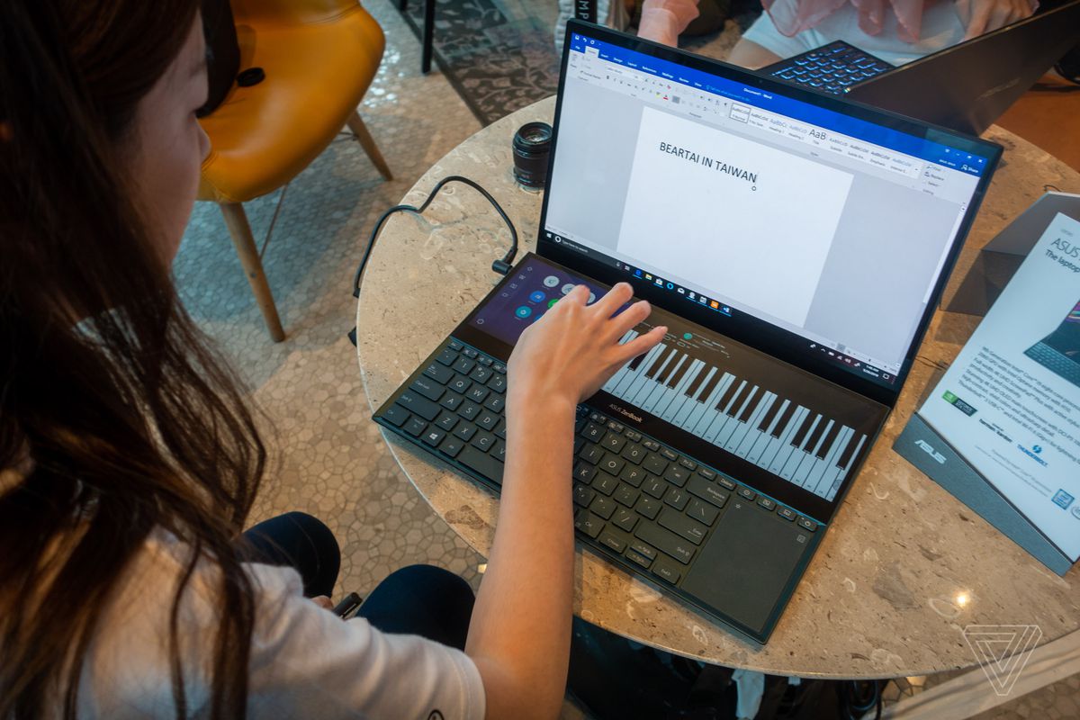
The ZenBook Pro Duo has not one, but two 4K screens. (At least if you’re counting horizontal pixels.) There’s a 15-inch 16:9 OLED panel where you’d normally find the display on a laptop, then a 32:9 IPS “ScreenPad Plus” screen directly above the keyboard that’s the same width and half the height. It’s as if Asus looked at the MacBook Pro Touch Bar and thought “what if that, but with 32 times as many pixels?”

Unlike the Touch Bar, though, the ScreenPad Plus doesn’t take anything away from the ZenBook Pro Duo, except presumably battery life. Asus still included a full-sized keyboard with a function row, including an escape key, and the trackpad is located directly to the right. The design is very reminiscent of Asus’ Zephryus slimline gaming laptops — you even still get the light-up etching that lets you use the trackpad as a numpad. HP tried something similar recently, too, though its second screen was far smaller.

asus

Asus has built some software for the ScreenPad Plus that makes it more of a secondary control panel, but you can also use it as a full-on monitor, or even two if you want to split it into two smaller 16:9 1080p windows. You can also set it to work as an extension of the main screen, so websites rise up from above your keyboard as you scroll down, which is pretty unnerving. Or you could use it to watch Lawrence of Arabia while you jam on Excel spreadsheets.

The ZenBook Pro Duo has up to an eight-core Intel Core i9 processor with an Nvidia RTX 2060 GPU. There are four far-field microphones designed for use with Alexa and Cortana, and there’s an Echo-style blue light at the bottom edge that activates with voice commands. It has a Thunderbolt 3 port, two USB-A ports, a headphone jack, and a full-sized HDMI port.

Performance seemed fine in my brief time using the ZenBook Pro Duo, without any hiccups or hitches even when running an intensive video editing software demo. It’s a fairly hefty laptop at 2.5kg (about 5.5lbs), but that’s to be expected given the gaming laptop-class internals. I would also expect its battery life to fall somewhere close to that particular category of products, though we’ll have to wait and see about that.

While both of the screens looked good, I will say they looked different. Part of that is because of the searing intensity of the primary OLED panel, but the ScreenPad Plus is also coated with a matte finish, and usually looks less bright because of how you naturally view it at an off angle.

asus

Asus is also making a cheaper and smaller 14-inch model called the ZenBook Duo. The design and concept is basically the same, but both screens are full HD rather than 4K, there’s no Core i9 option, and the discrete GPU has been heavily downgraded to an MX250.

Asus hasn’t announced pricing or availability for the ZenBook Pro Duo or the ZenBook Duo, but they’re expected to land in the third quarter of this year.

Source: The Asus ZenBook Pro Duo is an extravagant laptop with two 4K screens – The Verge

Why they see any similtarity to the Apple touch bar is beyond me – this is sprung from a totally different well. The dual screen laptop concept has been around for a lot longer than Apple putting a tiny strip somewhere. This is something that’s actually useful.

Tractors, not phones, will (maybe) get America a right-to-repair law at this rate: Bernie slams ‘truly insane’ situation

A person’s “right to repair” their own equipment may well become a US election issue, with presidential candidate Bernie Sanders making it a main talking point during his tour of Iowa.

“Are you ready for something truly insane?” the veteran politician’s account tweeted on Sunday, “Farmers aren’t allowed to repair their own tractors without paying an authorized John Deere repair agent.”

The tweet links to a clip of a recent Sanders rally during which he told the crowd to cheers: “Unbelievably, farmers are unable to even repair their own tractors, and tractors cost what – at least $150,000 – people are spending $150,000 for a piece of machinery. You know what I think? The person who buys that machinery has a right to fix the damn piece of machinery.”

The right-to-repair was also highlighted as one of Sanders’ key policies issues in his plan to “revitalize rural America,” and he promised: “When we are in the White House, we will pass a national right-to-repair law that gives every farmer in America full rights over the machinery they buy.”

Source: Tractors, not phones, will (maybe) get America a right-to-repair law at this rate: Bernie slams ‘truly insane’ situation • The Register

There is hope yet…

Aweigh – open source navigation system without satellites

Aweigh is an open navigation system that does not rely on satellites: it is inspired by the mapping of celestial bodies and the polarized vision of insects. Ancient seafarers and desert ants alike use universally accessible skylight to organize, orient, and place themselves in the world. Aweigh is a project that learns from the past and from the microscopic to re-position individuals in the contemporary technological landscape.

Networked technolgies that we increasingly rely on undergo changes that are often beyond our control. Most smartphone users require government-run satellites to get around day by day, while consequences of Brexit are calling into question the UK’s access to the EU’s new satellite system, Project Galileo. Aweigh is a set of tools and blueprints that aims to open modern technologies to means of democratization, dissemination, and self-determination.

These tools were designed to depend only on publicly available materials and resources: digital fabrication machines, open-source code, packaged instructions, and universally accessible sky light. Aweigh is inspired by ancient navigation devices that use the process of taking angular measurements between the earth and various celestial bodies as reference points to find one’s position. Combining this process with the polarization of sunlight observed in insect eyes, the group developed a technology that calculates longitude and latitude in urban as well as off-grid areas.

Source: Aweigh

Google and other tech giants are quietly buying up the most important part of the internet

In February, the company announced its intention to move forward with the development of the Curie cable, a new undersea line stretching from California to Chile. It will be the first private intercontinental cable ever built by a major non-telecom company.

And if you step back and just look at intracontinental cables, Google has fully financed a number of those already; it was one of the first companies to build a fully private submarine line.

Google isn’t alone. Historically, cables have been owned by groups of private companies — mostly telecom providers — but 2016 saw the start of a massive submarine cable boom, and this time, the buyers are content providers. Corporations like FacebookMicrosoft, and Amazon all seem to share Google’s aspirations for bottom-of-the-ocean dominance.

I’ve been watching this trend develop, being in the broadband space myself, and the recent movements are certainly concerning. Big tech’s ownership of the internet backbone will have far-reaching, yet familiar, implications. It’s the same old consumer tradeoff; more convenience for less control — and less privacy.

We’re reaching the next stage of internet maturity; one where only large, incumbent players can truly win in media.

[…]

If you want to measure the internet in miles, fiber-optic submarine cables are the place to start. These unassuming cables crisscross the ocean floor worldwide, carrying 95-99 percent of international data over bundles of fiber-optic cable strands the diameter of a garden hose. All told, there are more than 700,000 miles of submarine cables in use today.

[…]

Google will own 10,433 miles of submarine cables internationally when the Curie cable is completed later this year.

The total shoots up to 63,605 miles when you include cables it owns in consortium with Facebook, Microsoft, and Amazon

Source: Google and other tech giants are quietly buying up the most important part of the internet | VentureBeat

The hidden backdoor in Intel processors is a fascinating debug port (you have to pwner to use it anyway)

Researchers at the Black Hat Asia conference this week disclosed a previously unknown way to tap into the inner workings of Intel’s chip hardware.

The duo of Mark Ermolov and Maxim Goryachy from Positive Technologies explained how a secret Chipzilla system known as Visualization of Internal Signals Architecture (VISA) allows folks to peek inside the hidden workings and mechanisms of their CPU chipsets – capturing the traffic of individual signals and snapshots of the chip’s internal architecture in real time – without any special equipment.

To be clear, this hidden debug access is not really a security vulnerability. To utilize the channel, you must exploit a 2017 elevation-of-privilege vulnerability, or one similar to it, which itself requires you to have administrative or root-level access on the box. In other words, if an attacker can even get at VISA on your computer, it was already game over for you: they need admin rights.

Rather, Ermolov and Goryachy explained, the ability to access VISA will largely be of interest to researchers and chip designers who want to get a window into the lowest of the low-level operations of Chipzilla’s processor architecture.

What lies within

VISA is one of a set of hidden, non-publicly or partially publicly documented, interfaces called Trace Hub that Intel produced so that its engineers can see how data moves through the chips, and to help debug the flow of information between the processor and other hardware components. Specifically, the Platform Controller Hub, which hooks up CPU cores to the outside world of peripherals and other IO hardware, houses Trace Hub and VISA.

“This technology allows access to the internal CPU bus used to read and write memory,” the duo told The Register. “Using it, anyone now can investigate various aspects of hardware security: access control, internal addressing, and private configuration.”

Alongside VISA is an on-chip logic analyzer, and mechanisms for measuring architecture performance, inspecting security fuses, and monitoring things like speculative execution and out-of-order execution.

So, if the VISA controller isn’t much help to directly pwn someone else’s computer, where would it have use for non-Intel folks? Goryachy and Ermolov say that hardware hackers and researchers focused on the inner-workings of Intel chips would find VISA of great use when trying to suss out possible side-channel or speculative execution issues, secret security configurations, and so on.

“For example, the main issue while studying the speculative execution is getting feedback from the hardware,” they explained. “This technology provides an exact way to observe the internal state of the CPU or system-on-chip, and confirm any suppositions.”

The full slide presentation for the VISA system can be found on the Black Hat Asia website and demo videos are here. ®

Source: Ignore the noise about a scary hidden backdoor in Intel processors: It’s a fascinating debug port • The Register

Europe, Japan: D-Wave would really like you to play with its ‘2,000-qubit’ quantum Leap cloud service

Canadian startup D-Wave Systems has extended the availability of its Leap branded cloud-based quantum computing service to Europe and Japan.

With Leap, researchers will be granted free access to a live D-Wave 2000Q machine with – it is claimed – 2,000 quantum bits, or qubits.

Developers will also be free to use the company’s Quantum Application Environment, launched last year, which enables them to write quantum applications in Python.

Each D-Wave 2000Q normally costs around $15m.

It is important to note that the debate on whether D-Wave’s systems can be considered “true” quantum computers has raged since the company released its first commercial product in 2011.

Rather than focusing on maintaining its qubits in a coherent state – like Google, IBM and Intel – the company uses a process called quantum annealing to solve combinatorial optimisation problems. The process is less finnicky but also less useful, which is why D-Wave claims to offer a 2,000-qubit machine, and IBM presents a 20-qubit computer.

And yet D-Wave’s systems are being used by Google, NASA, Volkswagen, Lockheed Martin and BAE – as well as Oak Ridge and Los Alamos National Laboratories, among others.

Source: Europe, Japan: D-Wave would really like you to play with its – count ’em – ‘2,000-qubit’ quantum Leap cloud service • The Register

Microsoft just booted up the first “DNA drive” for storing data

Microsoft has helped build the first device that automatically encodes digital information into DNA and back to bits again.

DNA storage: Microsoft has been working toward a photocopier-size device that would replace data centers by storing files, movies, and documents in DNA strands, which can pack in information at mind-boggling density.

According to Microsoft, all the information stored in a warehouse-size data center would fit into a set of Yahztee dice, were it written in DNA.

Demo device: So far, DNA data storage has been carried out by hand in the lab. But now researchers at the University of Washington who are working with the software giant say they created a machine that converts electronic bits to DNA and back without a person involved.

The gadget, made from about $10,000 in parts, uses glass bottles of chemicals to build DNA strands, and a tiny sequencing machine from Oxford Nanopore to read them out again.

Still limited: According to a publication on March 21 in the journal Nature Scientific Reports, the team was able to store and retrieve just a single word—“hello”—or five bytes of data. What’s more, the process took 21 hours, mostly because of the slow chemical reactions involved in writing DNA.

While the team considered that a success for their prototype, a commercially useful DNA storage system would have to store data millions of times faster.

Why now? It’s a good time for companies involved in DNA storage to show off their stuff. The National Intelligence Agency’s IARPA program is getting ready to hand out tens of millions toward radical new molecular information storage schemes.

Source: Microsoft just booted up the first “DNA drive” for storing data – MIT Technology Review

Welding glass to metal breakthrough could transform manufacturing

Scientists from Heriot-Watt University have welded glass and metal together using an ultrafast laser system, in a breakthrough for the manufacturing industry.

Various optical materials such as quartz, borosilicate glass and even sapphire were all successfully welded to metals like aluminium, titanium and using the Heriot-Watt laser system, which provides very short, picosecond pulses of infrared light in tracks along the materials to fuse them together.

The new process could transform the and have direct applications in the aerospace, defence, optical technology and even healthcare fields.

Professor Duncan Hand, director of the five-university EPSRC Centre for Innovative Manufacturing in Laser-based Production Processes based at Heriot-Watt, said: “Traditionally it has been very difficult to weld together dissimilar materials like glass and metal due to their different thermal properties—the and highly different thermal expansions involved cause the glass to shatter.

“Being able to weld glass and metals together will be a huge step forward in manufacturing and design flexibility.

“At the moment, equipment and products that involve and metal are often held together by adhesives, which are messy to apply and parts can gradually creep, or move. Outgassing is also an issue—organic chemicals from the adhesive can be gradually released and can lead to reduced product lifetime.

“The process relies on the incredibly short pulses from the laser. These pulses last only a few picoseconds—a picosecond to a second is like a second compared to 30,000 years.

“The parts to be welded are placed in close contact, and the laser is focused through the optical material to provide a very small and highly intense spot at the interface between the two —we achieved megawatt peak power over an area just a few microns across.

“This creates a microplasma, like a tiny ball of lightning, inside the material, surrounded by a highly-confined melt region.

“We tested the welds at -50C to 90C and the welds remained intact, so we know they are robust enough to cope with extreme conditions.”

Read more at: https://phys.org/news/2019-03-welding-breakthrough.html#jCp

Source: Welding breakthrough could transform manufacturing

Physicists get thousands of semiconductor nuclei to do ‘quantum dances’ in unison

A team of Cambridge researchers have found a way to control the sea of nuclei in semiconductor quantum dots so they can operate as a quantum memory device.

Quantum dots are crystals made up of thousands of atoms, and each of these atoms interacts magnetically with the trapped electron. If left alone to its own devices, this interaction of the electron with the nuclear spins, limits the usefulness of the electron as a bit—a qubit.

Led by Professor Mete Atatüre, a Fellow at St John’s College, University of Cambridge, the research group, located at the Cavendish Laboratory, exploit the laws of quantum physics and optics to investigate computing, sensing or communication applications.

Atatüre said: “Quantum dots offer an ideal interface, as mediated by light, to a system where the dynamics of individual interacting spins could be controlled and exploited. Because the nuclei randomly ‘steal’ information from the electron they have traditionally been an annoyance, but we have shown we can harness them as a resource.”

The Cambridge team found a way to exploit the interaction between the electron and the thousands of nuclei using lasers to ‘cool’ the nuclei to less than 1 milliKelvin, or a thousandth of a degree above the absolute zero temperature. They then showed they can control and manipulate the thousands of nuclei as if they form a single body in unison, like a second qubit. This proves the nuclei in the quantum dot can exchange information with the electron qubit and can be used to store quantum information as a device. The findings have been published in Science today.

Quantum computing aims to harness fundamental concepts of quantum physics, such as entanglement and superposition principle, to outperform current approaches to computing and could revolutionise technology, business and research. Just like classical computers, quantum computers need a processor, memory, and a bus to transport the information backwards and forwards. The processor is a qubit which can be an electron trapped in a quantum dot, the bus is a single photon that these generate and are ideal for exchanging information. But the missing link for quantum dots is quantum memory.

Atatüre said: “Instead of talking to individual nuclear spins, we worked on accessing collective spin waves by lasers. This is like a stadium where you don’t need to worry about who raises their hands in the Mexican wave going round, as long as there is one collective wave because they all dance in unison.

“We then went on to show that these spin waves have quantum coherence. This was the missing piece of the jigsaw and we now have everything needed to build a dedicated quantum memory for every qubit.”

Read more at: https://phys.org/news/2019-02-physicists-thousands-semiconductor-nuclei-quantum.html#jCp

Source: Physicists get thousands of semiconductor nuclei to do ‘quantum dances’ in unison

Researchers develop smart micro-robots that can adapt to their surroundings

One day, hospital patients might be able to ingest tiny robots that deliver drugs directly to diseased tissue, thanks to research being carried out at EPFL and ETH Zurich.

A group of scientists led by Selman Sakar at EPFL and Bradley Nelson at ETH Zurich drew inspiration from bacteria to design smart, highly flexible biocompatible micro-robots. Because these devices are able to swim through fluids and modify their shape when needed, they can pass through narrow blood vessels and intricate systems without compromising on speed or maneuverability. They are made of hydrogel nanocomposites that contain magnetic , allowing them to be controlled via an .

In an article appearing in Science Advances, the scientists describe a method for programming the robot’s shape so that it can easily travel through fluids that are dense, viscous or moving at rapid speeds.

Embodied intelligence

Fabricating miniaturized robots presents a host of challenges, which the scientists addressed using an origami-based folding method. Their novel locomotion strategy employs embodied intelligence, which is an alternative to the classical computation paradigm that is performed by embedded electronic systems. “Our robots have a special composition and structure that allows them to adapt to the characteristics of the fluid they are moving through. For instance, if they encounter a change in viscosity or osmotic concentration, they modify their shape to maintain their speed and maneuverability without losing control of the direction of motion,” says Sakar.

Read more at: https://phys.org/news/2019-01-smart-micro-robots.html#jCp

Source: Researchers develop smart micro-robots that can adapt to their surroundings

An Amoeba-Based Computer Calculated Approximate Solutions to an 8 city Travelling Salesman Problem

A team of Japanese researchers from Keio University in Tokyo have demonstrated that an amoeba is capable of generating approximate solutions to a remarkably difficult math problem known as the “traveling salesman problem.”

The traveling salesman problem goes like this: Given an arbitrary number of cities and the distances between them, what is the shortest route a salesman can take that visits each city and returns to the salesman’s city of origin. It is a classic problem in computer science and is used as a benchmark test for optimization algorithms.

The traveling salesman problem is considered “NP hard,” which means that the complexity of calculating a correct solution increases exponentially the more cities are added to the problem. For example, there are only three possible solutions if there are four cities, but there are 360 possible solutions if there are six cities. It continues to increase exponentially from there.

Despite the exponential increase in computational difficulty with each city added to the salesman’s itinerary, computer scientists have been able to calculate the optimal solution to this problem for thousands of cities since the early 90s and recent efforts have been able to calculate nearly optimal solutions for millions of cities.

Amoebas are single-celled organisms without anything remotely resembling a central nervous system, which makes them seem like less than suitable candidates for solving such a complex puzzle. Yet as these Japanese researchers demonstrated, a certain type of amoeba can be used to calculate nearly optimal solutions to the traveling salesman problem for up to eight cities. Even more remarkably, the amount of time it takes the amoeba to reach these nearly optimal solutions grows linearly, even though the number of possible solutions increases exponentially.

As detailed in a paper published this week in Royal Society Open Science, the amoeba used by the researchers is called Physarum polycephalum, which has been used as a biological computer in several other experiments. The reason this amoeba is considered especially useful in biological computing is because it can extend various regions of its body to find the most efficient way to a food source and hates light.

To turn this natural feeding mechanism into a computer, the Japanese researcher placed the amoeba on a special plate that had 64 channels that it could extend its body into. This plate is then placed on top of a nutrient rich medium. The amoeba tries to extend its body to cover as much of the plate as possible and soak up the nutrients. Yet each channel in the plate can be illuminated, which causes the light-averse amoeba to retract from that channel.

To model the traveling salesman problem, each of the 64 channels on the plate was assigned a city code between A and H, in addition to a number from 1 to 8 that indicates the order of the cities. So, for example, if the amoeba extended its body into the channels A3, B2, C4, and D1, the correct solution to the traveling salesman problem would be D, B, A, C, D. The reason for this is that D1 indicates that D should be the first city in the salesman’s itinerary, B2 indicates B should be the second city, A3 that A should be the third city and so on.

To guide the amoeba toward a solution to the traveling salesman problem, the researchers used a neural network that would incorporate data about the amoeba’s current position and distance between the cities to light up certain channels. The neural network was designed such that cities with greater distances between them are more likely to be illuminated than channels that are not.

When the algorithm manipulates the chip that the amoeba is on it is basically coaxing it into taking forms that represent approximate solutions to the traveling salesman problem. As the researchers told Phys.org, they expect that it would be possible to manufacture chips that contain tens of thousands of channels so that the amoeba is able to solve traveling salesman problems that involve hundreds of cities.

For now, however, the Japanese researchers’ experiment remains in the lab, but it provides the foundation for low-energy biological computers that harness the natural mechanisms of amoebas and other microorganisms to compute.

Source: An Amoeba-Based Computer Calculated Approximate Solutions to a Very Hard Math Problem – Motherboard

Study opens route to ultra-low-power microchips

A new approach to controlling magnetism in a microchip could open the doors to memory, computing, and sensing devices that consume drastically less power than existing versions. The approach could also overcome some of the inherent physical limitations that have been slowing progress in this area until now.

Researchers at MIT and at Brookhaven National Laboratory have demonstrated that they can control the magnetic properties of a thin-film material simply by applying a small voltage. Changes in magnetic orientation made in this way remain in their new state without the need for any ongoing power, unlike today’s standard memory chips, the team has found.

The new finding is being reported today in the journal Nature Materials, in a paper by Geoffrey Beach, a professor of materials science and engineering and co-director of the MIT Materials Research Laboratory; graduate student Aik Jun Tan; and eight others at MIT and Brookhaven.

Source: Study opens route to ultra-low-power microchips | MIT News

Apple, Samsung fined in Italy for slowing people’s phones.

In a statement on Wednesday, the Italian competition authority, the Autorità Garante della Concorrenza e del Mercato (AGCM), said both companies had violated consumer protection laws by “inducing customers to install updates on devices that are not able to adequately support them.”

It fined Apple €10m ($11.4m): €5m for slowing down the iPhone 6 with its iOS 10 update, and a further €5m for not providing customers with sufficient information about their devices’ batteries, including how to maintain and replace them. Apple banks millions of dollars an hour in profit.

Samsung was fined €5m for its Android Marshmallow 6.0.1 update which was intended for the Galaxy Note 7 but which lead to the Note 4 malfunctioning due to the upgrade’s demands.

Both companies deny they deliberately set out to slow down older phones, but the Italian authorities were not persuaded and clearly felt it was a case of “built-in obsolescence” – where products are designed to fall apart before they need to in order to drive sales of newer models.

Source: Finally, someone takes a stand against Apple, Samsung for slowing people’s phones. Just a few million dollars, tho • The Register