Aweigh is an open navigation system that does not rely on satellites: it is inspired by the mapping of celestial bodies and the polarized vision of insects. Ancient seafarers and desert ants alike use universally accessible skylight to organize, orient, and place themselves in the world. Aweigh is a project that learns from the past and from the microscopic to re-position individuals in the contemporary technological landscape.
Networked technolgies that we increasingly rely on undergo changes that are often beyond our control. Most smartphone users require government-run satellites to get around day by day, while consequences of Brexit are calling into question the UK’s access to the EU’s new satellite system, Project Galileo. Aweigh is a set of tools and blueprints that aims to open modern technologies to means of democratization, dissemination, and self-determination.
These tools were designed to depend only on publicly available materials and resources: digital fabrication machines, open-source code, packaged instructions, and universally accessible sky light. Aweigh is inspired by ancient navigation devices that use the process of taking angular measurements between the earth and various celestial bodies as reference points to find one’s position. Combining this process with the polarization of sunlight observed in insect eyes, the group developed a technology that calculates longitude and latitude in urban as well as off-grid areas.
In February, the company announced its intention to move forward with the development of the Curie cable, a new undersea line stretching from California to Chile. It will be the first private intercontinental cable ever built by a major non-telecom company.
And if you step back and just look at intracontinental cables, Google has fully financed a number of those already; it was one of the first companies to build a fully private submarine line.
Google isn’t alone. Historically, cables have been owned by groups of private companies — mostly telecom providers — but 2016 saw the start of a massive submarine cable boom, and this time, the buyers are content providers. Corporations like Facebook, Microsoft, and Amazon all seem to share Google’s aspirations for bottom-of-the-ocean dominance.
I’ve been watching this trend develop, being in the broadband space myself, and the recent movements are certainly concerning. Big tech’s ownership of the internet backbone will have far-reaching, yet familiar, implications. It’s the same old consumer tradeoff; more convenience for less control — and less privacy.
We’re reaching the next stage of internet maturity; one where only large, incumbent players can truly win in media.
[…]
If you want to measure the internet in miles, fiber-optic submarine cables are the place to start. These unassuming cables crisscross the ocean floor worldwide, carrying 95-99 percent of international data over bundles of fiber-optic cable strands the diameter of a garden hose. All told, there are more than 700,000 miles of submarine cables in use today.
[…]
Google will own 10,433 miles of submarine cables internationally when the Curie cable is completed later this year.
The total shoots up to 63,605 miles when you include cables it owns in consortium with Facebook, Microsoft, and Amazon
Researchers at the Black Hat Asia conference this week disclosed a previously unknown way to tap into the inner workings of Intel’s chip hardware.
The duo of Mark Ermolov and Maxim Goryachy from Positive Technologies explained how a secret Chipzilla system known as Visualization of Internal Signals Architecture (VISA) allows folks to peek inside the hidden workings and mechanisms of their CPU chipsets – capturing the traffic of individual signals and snapshots of the chip’s internal architecture in real time – without any special equipment.
To be clear, this hidden debug access is not really a security vulnerability. To utilize the channel, you must exploit a 2017 elevation-of-privilege vulnerability, or one similar to it, which itself requires you to have administrative or root-level access on the box. In other words, if an attacker can even get at VISA on your computer, it was already game over for you: they need admin rights.
Rather, Ermolov and Goryachy explained, the ability to access VISA will largely be of interest to researchers and chip designers who want to get a window into the lowest of the low-level operations of Chipzilla’s processor architecture.
What lies within
VISA is one of a set of hidden, non-publicly or partially publicly documented, interfaces called Trace Hub that Intel produced so that its engineers can see how data moves through the chips, and to help debug the flow of information between the processor and other hardware components. Specifically, the Platform Controller Hub, which hooks up CPU cores to the outside world of peripherals and other IO hardware, houses Trace Hub and VISA.
“This technology allows access to the internal CPU bus used to read and write memory,” the duo told The Register. “Using it, anyone now can investigate various aspects of hardware security: access control, internal addressing, and private configuration.”
Alongside VISA is an on-chip logic analyzer, and mechanisms for measuring architecture performance, inspecting security fuses, and monitoring things like speculative execution and out-of-order execution.
So, if the VISA controller isn’t much help to directly pwn someone else’s computer, where would it have use for non-Intel folks? Goryachy and Ermolov say that hardware hackers and researchers focused on the inner-workings of Intel chips would find VISA of great use when trying to suss out possible side-channel or speculative execution issues, secret security configurations, and so on.
“For example, the main issue while studying the speculative execution is getting feedback from the hardware,” they explained. “This technology provides an exact way to observe the internal state of the CPU or system-on-chip, and confirm any suppositions.”
Canadian startup D-Wave Systems has extended the availability of its Leap branded cloud-based quantum computing service to Europe and Japan.
With Leap, researchers will be granted free access to a live D-Wave 2000Q machine with – it is claimed – 2,000 quantum bits, or qubits.
Developers will also be free to use the company’s Quantum Application Environment, launched last year, which enables them to write quantum applications in Python.
It is important to note that the debate on whether D-Wave’s systems can be considered “true” quantum computers has raged since the company released its first commercial product in 2011.
Rather than focusing on maintaining its qubits in a coherent state – like Google, IBM and Intel – the company uses a process called quantum annealing to solve combinatorial optimisation problems. The process is less finnicky but also less useful, which is why D-Wave claims to offer a 2,000-qubit machine, and IBM presents a 20-qubit computer.
And yet D-Wave’s systems are being used by Google, NASA, Volkswagen, Lockheed Martin and BAE – as well as Oak Ridge and Los Alamos National Laboratories, among others.
Microsoft has helped build the first device that automatically encodes digital information into DNA and back to bits again.
DNA storage: Microsoft has been working toward a photocopier-size device that would replace data centers by storing files, movies, and documents in DNA strands, which can pack in information at mind-boggling density.
According to Microsoft, all the information stored in a warehouse-size data center would fit into a set of Yahztee dice, were it written in DNA.
Demo device: So far, DNA data storage has been carried out by hand in the lab. But now researchers at the University of Washington who are working with the software giant say they created a machine that converts electronic bits to DNA and back without a person involved.
The gadget, made from about $10,000 in parts, uses glass bottles of chemicals to build DNA strands, and a tiny sequencing machine from Oxford Nanopore to read them out again.
Still limited: According to a publication on March 21 in the journal Nature Scientific Reports, the team was able to store and retrieve just a single word—“hello”—or five bytes of data. What’s more, the process took 21 hours, mostly because of the slow chemical reactions involved in writing DNA.
While the team considered that a success for their prototype, a commercially useful DNA storage system would have to store data millions of times faster.
Why now? It’s a good time for companies involved in DNA storage to show off their stuff. The National Intelligence Agency’s IARPA program is getting ready to hand out tens of millions toward radical new molecular information storage schemes.
Scientists from Heriot-Watt University have welded glass and metal together using an ultrafast laser system, in a breakthrough for the manufacturing industry.
Various optical materials such as quartz, borosilicate glass and even sapphire were all successfully welded to metals like aluminium, titanium and stainless steel using the Heriot-Watt laser system, which provides very short, picosecond pulses of infrared light in tracks along the materials to fuse them together.
The new process could transform the manufacturing sector and have direct applications in the aerospace, defence, optical technology and even healthcare fields.
Professor Duncan Hand, director of the five-university EPSRC Centre for Innovative Manufacturing in Laser-based Production Processes based at Heriot-Watt, said: “Traditionally it has been very difficult to weld together dissimilar materials like glass and metal due to their different thermal properties—the high temperatures and highly different thermal expansions involved cause the glass to shatter.
“Being able to weld glass and metals together will be a huge step forward in manufacturing and design flexibility.
“At the moment, equipment and products that involve glass and metal are often held together by adhesives, which are messy to apply and parts can gradually creep, or move. Outgassing is also an issue—organic chemicals from the adhesive can be gradually released and can lead to reduced product lifetime.
“The process relies on the incredibly short pulses from the laser. These pulses last only a few picoseconds—a picosecond to a second is like a second compared to 30,000 years.
“The parts to be welded are placed in close contact, and the laser is focused through the optical material to provide a very small and highly intense spot at the interface between the two materials—we achieved megawatt peak power over an area just a few microns across.
“This creates a microplasma, like a tiny ball of lightning, inside the material, surrounded by a highly-confined melt region.
“We tested the welds at -50C to 90C and the welds remained intact, so we know they are robust enough to cope with extreme conditions.”
A team of Cambridge researchers have found a way to control the sea of nuclei in semiconductor quantum dots so they can operate as a quantum memory device.
Quantum dots are crystals made up of thousands of atoms, and each of these atoms interacts magnetically with the trapped electron. If left alone to its own devices, this interaction of the electron with the nuclear spins, limits the usefulness of the electron as a quantum bit—a qubit.
Led by Professor Mete Atatüre, a Fellow at St John’s College, University of Cambridge, the research group, located at the Cavendish Laboratory, exploit the laws of quantum physics and optics to investigate computing, sensing or communication applications.
Atatüre said: “Quantum dots offer an ideal interface, as mediated by light, to a system where the dynamics of individual interacting spins could be controlled and exploited. Because the nuclei randomly ‘steal’ information from the electron they have traditionally been an annoyance, but we have shown we can harness them as a resource.”
The Cambridge team found a way to exploit the interaction between the electron and the thousands of nuclei using lasers to ‘cool’ the nuclei to less than 1 milliKelvin, or a thousandth of a degree above the absolute zero temperature. They then showed they can control and manipulate the thousands of nuclei as if they form a single body in unison, like a second qubit. This proves the nuclei in the quantum dot can exchange information with the electron qubit and can be used to store quantum information as a memory device. The findings have been published in Science today.
Quantum computing aims to harness fundamental concepts of quantum physics, such as entanglement and superposition principle, to outperform current approaches to computing and could revolutionise technology, business and research. Just like classical computers, quantum computers need a processor, memory, and a bus to transport the information backwards and forwards. The processor is a qubit which can be an electron trapped in a quantum dot, the bus is a single photon that these quantum dots generate and are ideal for exchanging information. But the missing link for quantum dots is quantum memory.
Atatüre said: “Instead of talking to individual nuclear spins, we worked on accessing collective spin waves by lasers. This is like a stadium where you don’t need to worry about who raises their hands in the Mexican wave going round, as long as there is one collective wave because they all dance in unison.
“We then went on to show that these spin waves have quantum coherence. This was the missing piece of the jigsaw and we now have everything needed to build a dedicated quantum memory for every qubit.”
One day, hospital patients might be able to ingest tiny robots that deliver drugs directly to diseased tissue, thanks to research being carried out at EPFL and ETH Zurich.
A group of scientists led by Selman Sakar at EPFL and Bradley Nelson at ETH Zurich drew inspiration from bacteria to design smart, highly flexible biocompatible micro-robots. Because these devices are able to swim through fluids and modify their shape when needed, they can pass through narrow blood vessels and intricate systems without compromising on speed or maneuverability. They are made of hydrogel nanocomposites that contain magnetic nanoparticles, allowing them to be controlled via an electromagnetic field.
In an article appearing in Science Advances, the scientists describe a method for programming the robot’s shape so that it can easily travel through fluids that are dense, viscous or moving at rapid speeds.
Embodied intelligence
Fabricating miniaturized robots presents a host of challenges, which the scientists addressed using an origami-based folding method. Their novel locomotion strategy employs embodied intelligence, which is an alternative to the classical computation paradigm that is performed by embedded electronic systems. “Our robots have a special composition and structure that allows them to adapt to the characteristics of the fluid they are moving through. For instance, if they encounter a change in viscosity or osmotic concentration, they modify their shape to maintain their speed and maneuverability without losing control of the direction of motion,” says Sakar.
A team of Japanese researchers from Keio University in Tokyo have demonstrated that an amoeba is capable of generating approximate solutions to a remarkably difficult math problem known as the “traveling salesman problem.”
The traveling salesman problem goes like this: Given an arbitrary number of cities and the distances between them, what is the shortest route a salesman can take that visits each city and returns to the salesman’s city of origin. It is a classic problem in computer science and is used as a benchmark test for optimization algorithms.
The traveling salesman problem is considered “NP hard,” which means that the complexity of calculating a correct solution increases exponentially the more cities are added to the problem. For example, there are only three possible solutions if there are four cities, but there are 360 possible solutions if there are six cities. It continues to increase exponentially from there.
Despite the exponential increase in computational difficulty with each city added to the salesman’s itinerary, computer scientists have been able to calculate the optimal solution to this problem for thousands of cities since the early 90s and recent efforts have been able to calculate nearly optimal solutions for millions of cities.
Amoebas are single-celled organisms without anything remotely resembling a central nervous system, which makes them seem like less than suitable candidates for solving such a complex puzzle. Yet as these Japanese researchers demonstrated, a certain type of amoeba can be used to calculate nearly optimal solutions to the traveling salesman problem for up to eight cities. Even more remarkably, the amount of time it takes the amoeba to reach these nearly optimal solutions grows linearly, even though the number of possible solutions increases exponentially.
As detailed in a paper published this week in Royal Society Open Science, the amoeba used by the researchers is called Physarum polycephalum, which has been used as a biological computer in several other experiments. The reason this amoeba is considered especially useful in biological computing is because it can extend various regions of its body to find the most efficient way to a food source and hates light.
To turn this natural feeding mechanism into a computer, the Japanese researcher placed the amoeba on a special plate that had 64 channels that it could extend its body into. This plate is then placed on top of a nutrient rich medium. The amoeba tries to extend its body to cover as much of the plate as possible and soak up the nutrients. Yet each channel in the plate can be illuminated, which causes the light-averse amoeba to retract from that channel.
To model the traveling salesman problem, each of the 64 channels on the plate was assigned a city code between A and H, in addition to a number from 1 to 8 that indicates the order of the cities. So, for example, if the amoeba extended its body into the channels A3, B2, C4, and D1, the correct solution to the traveling salesman problem would be D, B, A, C, D. The reason for this is that D1 indicates that D should be the first city in the salesman’s itinerary, B2 indicates B should be the second city, A3 that A should be the third city and so on.
To guide the amoeba toward a solution to the traveling salesman problem, the researchers used a neural network that would incorporate data about the amoeba’s current position and distance between the cities to light up certain channels. The neural network was designed such that cities with greater distances between them are more likely to be illuminated than channels that are not.
When the algorithm manipulates the chip that the amoeba is on it is basically coaxing it into taking forms that represent approximate solutions to the traveling salesman problem. As the researchers told Phys.org, they expect that it would be possible to manufacture chips that contain tens of thousands of channels so that the amoeba is able to solve traveling salesman problems that involve hundreds of cities.
For now, however, the Japanese researchers’ experiment remains in the lab, but it provides the foundation for low-energy biological computers that harness the natural mechanisms of amoebas and other microorganisms to compute.
A new approach to controlling magnetism in a microchip could open the doors to memory, computing, and sensing devices that consume drastically less power than existing versions. The approach could also overcome some of the inherent physical limitations that have been slowing progress in this area until now.
Researchers at MIT and at Brookhaven National Laboratory have demonstrated that they can control the magnetic properties of a thin-film material simply by applying a small voltage. Changes in magnetic orientation made in this way remain in their new state without the need for any ongoing power, unlike today’s standard memory chips, the team has found.
The new finding is being reported today in the journal Nature Materials, in a paper by Geoffrey Beach, a professor of materials science and engineering and co-director of the MIT Materials Research Laboratory; graduate student Aik Jun Tan; and eight others at MIT and Brookhaven.
In a statement on Wednesday, the Italian competition authority, the Autorità Garante della Concorrenza e del Mercato (AGCM), said both companies had violated consumer protection laws by “inducing customers to install updates on devices that are not able to adequately support them.”
It fined Apple €10m ($11.4m): €5m for slowing down the iPhone 6 with its iOS 10 update, and a further €5m for not providing customers with sufficient information about their devices’ batteries, including how to maintain and replace them. Apple banks millions of dollars an hour in profit.
Samsung was fined €5m for its Android Marshmallow 6.0.1 update which was intended for the Galaxy Note 7 but which lead to the Note 4 malfunctioning due to the upgrade’s demands.
Both companies deny they deliberately set out to slow down older phones, but the Italian authorities were not persuaded and clearly felt it was a case of “built-in obsolescence” – where products are designed to fall apart before they need to in order to drive sales of newer models.
Why is Xiaomi’s fitness tracker detecting a heartbeat from a roll of toilet paper?
Weibo users are confused, but the answer isn’t as wild as it seems
Does a roll of toilet paper have a heart? Obviously not. So why does Xiaomi’s fitness band display a heart rate when it’s wrapped around a roll of toilet paper?
Weibo users have been discussing the phenomenon, with plenty of pictures from mystified users who say the Xiaomi Mi Band 3 fitness tracker is “detecting” a heart rate on toilet paper.
So we decided to get a Mi Band 3 — and of course, a roll of toilet paper — to check it out.
Bizarrely, it’s true.
It didn’t work all the time — only around a quarter of attempts gave us a heartbeat. The numbers were pretty random (ranging from 59bpm to 88bpm), but they were real.
So what about other objects? We tried wrapping the Mi Band 3 around a mug, because we had a mug, and a banana, because the internet likes bananas. Both gave us a heart rate quickly and far more consistently than the toilet paper did.
59bpm? That roll of toilet paper is so chill right now. (Picture: Abacus)
But the Xiaomi band isn’t alone. We also tried the banana and mug with an Apple Watch Series 4 and a Ticwatch, an Android Wear smartwatch. Both also displayed a heartbeat for the two heartless objects, ranging from 33bpm on the banana (Apple Watch) to 130bpm for the mug (Ticwatch).
Researchers from Linköping University and the Royal Institute of Technology in Sweden have proposed a new device concept that can efficiently transfer the information carried by electron spin to light at room temperature—a stepping stone toward future information technology. They present their approach in an article in Nature Communications.
Light and electron charge are the main media for information processing and transfer. In the search for information technology that is even faster, smaller and more energy-efficient, scientists around the globe are exploring another property of electrons—their spin. Electronics that exploit both the spin and the charge of the electron are called “spintronics.”
[…]
“The main problem is that electrons easily lose their spin orientations when the temperature rises. A key element for future spin-light applications is efficient quantum information transfer at room temperature, but at room temperature, the electron spin orientation is nearly randomized.
[…]
Now, researchers from Linköping University and the Royal Institute of Technology have devised an efficient spin-light interface.
“This interface can not only maintain and even enhance the electron spin signals at room temperature. It can also convert these spin signals to corresponding chiral light signals travelling in a desired direction,” says Weimin Chen.
The key element of the device is extremely small disks of gallium nitrogen arsenide, GaNAs. The disks are only a couple of nanometres high and stacked on top of each other with a thin layer of gallium arsenide (GaAs) between to form chimney-shaped nanopillars. For comparison, the diameter of a human hair is about a thousand times larger than the diameter of the nanopillars.
The unique ability of the proposed device to enhance spin signals is due to minimal defects introduced into the material by the researchers. Fewer than one out of a million gallium atoms are displaced from their designated lattice sites in the material. The resulting defects in the material act as efficient spin filters that can drain electrons with an unwanted spin orientation and preserve those with the desired spin orientation.
“An important advantage of the nanopillar design is that light can be guided easily and more efficiently coupled in and out,” says Shula Chen, first author of the article.
Over on the EEVblog, someone noticed an interesting chip that’s been apparently flying under our radar for a while. This is an ARM processor capable of running Linux. It’s hand-solderable in a TQFP package, has a built-in Mali GPU, support for a touch panel, and has support for 512MB of DDR3. If you do it right, this will get you into the territory of a BeagleBone or a Raspberry Pi Zero, on a board that’s whatever form factor you can imagine. Here’s the best part: you can get this part for $1 USD in large-ish quantities. A cursory glance at the usual online retailers tells me you can get this part in quantity one for under $3. This is interesting, to say the least.
The chip in question, the Allwinner A13, is a 1GHz ARM Cortex-A8 processor. While it’s not much, it is a chip that can run Linux in a hand-solderable package. There is no HDMI support, you’ll need to add some more chips (that are probably in a BGA package), but, hey, it’s only a dollar.
If you’d like to prototype with this chip, the best options right now are a few boards from Olimex, and a System on Module from the same company. That SoM is an interesting bit of kit, allowing anyone to connect a power supply, load an SD card, and get this chip doing something.
Currently, there aren’t really any good solutions for a cheap Linux system you can build at home, with hand-solderable chips. Yes, you could put Linux on an ATMega, but that’s the worst PC ever. A better option is the Octavo OSD335x SoC, better known as ‘the BeagleBone on a Chip’. This is a BGA chip, but the layout isn’t too bad, and it can be assembled using a $12 toaster oven. The problem with this chip is the price; at quantity 1000, it’s a $25 chip. At quantity one, it’s a $40 chip. NXP’s i.MX6 chips have great software support, but they’re $30 chips, and you’ll need some DDR to make it do something useful, and that doesn’t even touch the fiddlyness of a 600-ball package
While the Allwinner A13 beats all the other options on price and solderability, it should be noted that like all of these random Linux-capable SoCs, the software is a mess. There is a reason those ‘Raspberry Pi killers’ haven’t yet killed the Raspberry Pi, and it’s because the Allwinner chips don’t have documentation and let’s repeat that for emphasis: the software is a mess.
Metals are widely used for antennas; however, their bulkiness limits the fabrication of thin, lightweight, and flexible antennas. Recently, nanomaterials such as graphene, carbon nanotubes, and conductive polymers came into play. However, poor conductivity limits their use. We show RF devices for wireless communication based on metallic two-dimensional (2D) titanium carbide (MXene) prepared by a single-step spray coating. We fabricated a ~100-nm-thick translucent MXene antenna with a reflection coefficient of less than −10 dB. By increasing the antenna thickness to 8 μm, we achieved a reflection coefficient of −65 dB. We also fabricated a 1-μm-thick MXene RF identification device tag reaching a reading distance of 8 m at 860 MHz. Our finding shows that 2D titanium carbide MXene operates below the skin depth of copper or other metals as well as offers an opportunity to produce transparent antennas.
Lenovo is making it easier for their customers running Linux to update their firmware now on ThinkPad, ThinkStation, and ThinkCenter hardware.
Lenovo has joined the Linux Vendor Firmware Service (LVFS) and following collaboration with the upstream developers is beginning to roll-out support for offering their device firmware on this platform so it can be easily updated by users with the fwupd stack. Kudos to all involved especially with Lenovo ThinkPads being very popular among Linux users.
Red Hat’s Richard Hughes outlined the Lenovo collaboration on his blog and more Lenovo device firmware will begin appearing on LVFS in the next few weeks.
In his post, Richard also called out HP as now being one of the few major vendors not yet officially backing the LVFS.
There are, to date, seven different HDMI versions, starting with 1.0, which was introduced back in 2002, and currently ending with 2.1, which was only announced back in November of 2017. The amount of bandwidth each each version is capable of supporting, as well as any additional cool features a version may possess, is decided upon by the HDMI licensing group, which is made of a collection of companies, including Toshiba, Technicolor, Panasonic and Sony.
HDMI Version 1.4, which was introduced back in 2009, is the current de facto standard HDMI cable. It supports up to 10Gbps and a 1080p resolution with a 120Hz refresh rate (which means the screen can display 120 frames per second—great for sports and games), but it can only do 4K at 60Hz, and it can’t handle new features like HDR and wide color gamut. That means it’s worthless if you’re trying to hook up the latest set-top box or game console with most TVs made in the last two to three years.
Well, it’s not worthless, but it’s not ideal, either! You’re essentially losing out on the cool features you paid for in that TV and HDMI-connected device.
HDMI 1.4 also has to sub versions: 1.4a and 1.4b. The former allows the cable to work with 3D televisions in 1080p 24Hz, and the latter allows it to also handle 3D 1080p at 120Hz. Neither provides any noticeable improvement if you’re using one with a 2D television. As 3D TVs aren’t especially popular anymore, and there’s not a lot of content available, you don’t really need to think too much about these two—they’ll still work just like a vanilla version 1.4 cable.
What does provide an improvement is moving to Version 2.0. With this upgrade, the maximum bandwidth of the cable nearly doubles, from 10Gbps to 18Gbps. This means the cable can theoretically transmit a lot more data—like all the data needed to properly render a wider color gamut or HDR. Unfortunately, you’re still capped at 4K and 60Hz. So if you head into the big box store and they try to sell you on a fancy 4K TV capable of 120Hz, don’t necessarily feel like you need to spend the money. You will not be able to get a 4K 120Hz picture transmitted over HDMI with version 2.0 or earlier.
This might be where you point to Version 2.1, which was announced back in November 2017. It doesn’t just double the bandwidth. At a theoretical max of 48Gbps, it’s almost three times faster than 2.0 and nearly five times faster than 1.4 or earlier. It can actually do 4K and 120Hz and wide color gamut and HDR all at the same time. However, because it was announced in November 2017, there are very, very few TVs with ports that support the standard, or cables made to the standard.
HDMI cable standards are hidden, because the world is terrible
At this point, you might think you cracked the code, as if you could just go out, find an HDMI 2.0 or 2.1 cable, plug it in, and you’re good to go. Unfortunately, in 2012 HDMI pulled a truly bonehead move and essentially forbid anyone from actually saying what standards their cables support.
You can’t just go to Monoprice or Amazon and choose a nice-looking 2.0 cable and call it a day. But thankfully this guide exists, so you also don’t have to pore over every single number that chases after an HDMI cable when you do a search on Monoprice or Amazon.
The key thing isn’t to look for 4K, or 60Hz, or HDR, or more complex stats like YUV 4:4:4. All you actually need to pay attention to is the bandwidth of the cable. You want to find cables that say they are capable of 18Gbps or higher.
You also want to make sure that those cables are certified, as uncertified cables can make any kind of bandwidth claim they please and not actually deliver. A certified cable will be a little more expensive, but that means a dollar or two more. It’s a small price to pay to make sure your $1,000 TV is showing the picture it was designed to show.
Knowing when to trash a cable
So how do you know if the cables you already have are worthless? There typically aren’t any markers on the cable you can trust to accurately tell you. So if you don’t want to chuck all the cables you currently own and go buy all new ones, you’ll need to check a few things.
First, look at the manual for you TV and see what version of HDMI each port supports. Many TVs, especially cheaper ones, might only have Version 2.0 or higher on one port! That means there’s only one port that can handle 4K and HDR and all the stuff the TV bragged about having when you bought it. So locate a Version 2.0 port on your TV and plug in a device that supports 4K and HDR. Now, confirm that HDR is enabled on the TV. You’ll need to check you manual as every TV confirms HDR differently.
If HDR is enabled then you’re probably good to go! But if it is enabled and you notice the picture is pixelating or stuttering, then it means the cable can’t handle all the data and should be replaced. This is especially common with cables over 6 feet that are attempting to transmit 4K 60Hz picture with wide color gamut and HDR. For that reason, it’s rarely a good idea to buy a cable that is longer than 6 feet.
As good certified cables can be found at places like Amazon and Monoprice for under $10, there’s really no reason not to double-check and replace your cables if needed. You spent all that money on a good picture, so why waste it because of a cheap cable?
Nvidia’s flagship Titan V graphics cards may have hardware gremlins causing them to spit out different answers to repeated complex calculations under certain conditions, according to computer scientists.
The Titan V is the Silicon Valley giant’s most powerful GPU board available to date, and is built on Nv’s Volta technology. Gamers and casual users will not notice any errors or issues, however folks running intensive scientific software may encounter occasional glitches.
One engineer told The Register that when he tried to run identical simulations of an interaction between a protein and enzyme on Nvidia’s Titan V cards, the results varied. After repeated tests on four of the top-of-the-line GPUs, he found two gave numerical errors about 10 per cent of the time. These tests should produce the same output values each time again and again. On previous generations of Nvidia hardware, that generally was the case. On the Titan V, not so, we’re told.
We have repeatedly asked Nvidia for an explanation, and spokespeople have declined to comment. With Nvidia kicking off its GPU Technology Conference in San Jose, California, next week, perhaps then we’ll get some answers.
All in all, it is bad news for boffins as reproducibility is essential to scientific research. When running a physics simulation, any changes from one run to another should be down to interactions within the virtual world, not rare glitches in the underlying hardware.
[…]
Unlike previous GeForce and Titan GPUs, the Titan V is geared not so much for gamers but for handling intensive parallel computing workloads for data science, modeling, and machine learning.
And at $2,999 (£2,200) a pop, it’s not cheap to waste resources and research time on faulty hardware. Engineers speaking to The Register on condition of anonymity to avoid repercussions from Nvidia said the best solution to these problems is to avoid using Titan V altogether until a software patch has been released to address the mathematical oddities.
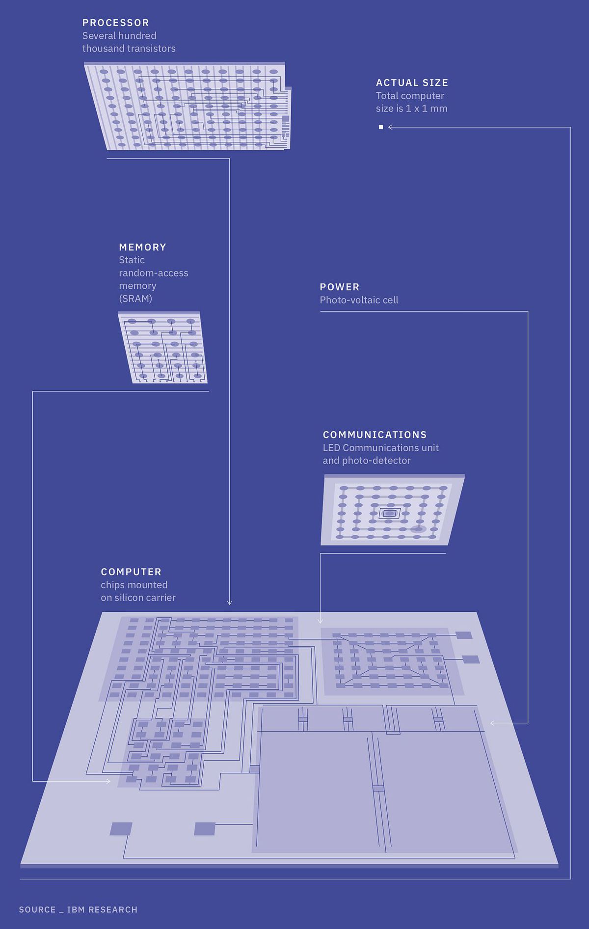
March 19 is the first day of IBM Think 2018, the company’s flagship conference, where the company will unveil what it claims is the world’s smallest computer. They’re not kidding: It’s literally smaller than a grain of salt.
But don’t let the size fool you: This sucker has the computing power of the x86 chip from 1990. Okay, so that’s not great compared to what we have today, but cut it some slack — you need a microscope to see it.
The computer will cost less than ten cents to manufacture, and will also pack “several hundred thousand transistors,” according to the company. These will allow it to “monitor, analyze, communicate, and even act on data.”
[…]
According to IBM, this is only the beginning. “Within the next five years, cryptographic anchors — such as ink dots or tiny computers smaller than a grain of salt — will be embedded in everyday objects and devices,” says IBM head of research Arvind Krishna. If he’s correct, we’ll see way more of these tiny systems in objects and devices in the years to come.
It is not much to look at: the nematode C. elegans is about one millimetre in length and is a very simple organism. But for science, it is extremely interesting. C. elegans is the only living being whose neural system has been analysed completely. It can be drawn as a circuit diagram or reproduced by computer software, so that the neural activity of the worm is simulated by a computer program.
Such an artificial C. elegans has now been trained at TU Wien (Vienna) to perform a remarkable trick: The computer worm has learned to balance a pole at the tip of its tail.
[…]
“With the help of reinforcement learning, a method also known as ‘learning based on experiment and reward’, the artificial reflex network was trained and optimized on the computer”, Mathias Lechner explains. And indeed, the team succeeded in teaching the virtual nerve system to balance a pole. “The result is a controller, which can solve a standard technology problem – stabilizing a pole, balanced on its tip. But no human being has written even one line of code for this controller, it just emerged by training a biological nerve system”, says Radu Grosu.
The team is going to explore the capabilities of such control-circuits further. The project raises the question, whether there is a fundamental difference between living nerve systems and computer code. Is machine learning and the activity of our brain the same on a fundamental level? At least we can be pretty sure that the simple nematode C. elegans does not care whether it lives as a worm in the ground or as a virtual worm on a computer hard drive.
Razer is a vendor that makes high-end gaming hardware, including laptops, keyboards and mice. I opened a ticket with Razor a few days ago asking them if they wanted to support the LVFS project by uploading firmware and sharing the firmware update protocol used. I offered to upstream any example code they could share under a free license, or to write the code from scratch given enough specifications to do so. This is something I’ve done for other vendors, and doesn’t take long as most vendor firmware updaters all do the same kind of thing; there are only so many ways to send a few kb of data to USB devices. The fwupd project provides high-level code for accessing USB devices, so yet-another-update-protocol is no big deal. I explained all about the LVFS, and the benefits it provided to a userbase that is normally happy to vote using their wallet to get hardware that’s supported on the OS of their choice.
I just received this note on the ticket, which was escalated appropriately:
I have discussed your offer with the dedicated team and we are thankful for your enthusiasm and for your good idea.
I am afraid I have also to let you know that at this moment in time our support for software is only focused on Windows and Mac.
The CEO of Razer Min-Liang Tan said recently “We’re inviting all Linux enthusiasts to weigh in at the new Linux Corner on Insider to post feedback, suggestions and ideas on how we can make it the best notebook in the world that supports Linux.” If this is true, and more than just a sound-bite, supporting the LVFS for firmware updates on the Razer Blade to solve security problems like Meltdown and Spectre ought to be a priority?
I have gone off them since they require their products to be connected via their cloud to change settings and receive updates. There is absolutely no reason for a mouse to need to be connected to Razer to change settings.
engineers at MIT have designed an artificial synapse in such a way that they can precisely control the strength of an electric current flowing across it, similar to the way ions flow between neurons. The team has built a small chip with artificial synapses, made from silicon germanium. In simulations, the researchers found that the chip and its synapses could be used to recognize samples of handwriting, with 95 percent accuracy.
[…]
Most neuromorphic chip designs attempt to emulate the synaptic connection between neurons using two conductive layers separated by a “switching medium,” or synapse-like space. When a voltage is applied, ions should move in the switching medium to create conductive filaments, similarly to how the “weight” of a synapse changes.
But it’s been difficult to control the flow of ions in existing designs. Kim says that’s because most switching mediums, made of amorphous materials, have unlimited possible paths through which ions can travel — a bit like Pachinko, a mechanical arcade game that funnels small steel balls down through a series of pins and levers, which act to either divert or direct the balls out of the machine.
Like Pachinko, existing switching mediums contain multiple paths that make it difficult to predict where ions will make it through. Kim says that can create unwanted nonuniformity in a synapse’s performance.
“Once you apply some voltage to represent some data with your artificial neuron, you have to erase and be able to write it again in the exact same way,” Kim says. “But in an amorphous solid, when you write again, the ions go in different directions because there are lots of defects. This stream is changing, and it’s hard to control. That’s the biggest problem — nonuniformity of the artificial synapse.”
A perfect mismatch
Instead of using amorphous materials as an artificial synapse, Kim and his colleagues looked to single-crystalline silicon, a defect-free conducting material made from atoms arranged in a continuously ordered alignment. The team sought to create a precise, one-dimensional line defect, or dislocation, through the silicon, through which ions could predictably flow.
To do so, the researchers started with a wafer of silicon, resembling, at microscopic resolution, a chicken-wire pattern. They then grew a similar pattern of silicon germanium — a material also used commonly in transistors — on top of the silicon wafer. Silicon germanium’s lattice is slightly larger than that of silicon, and Kim found that together, the two perfectly mismatched materials can form a funnel-like dislocation, creating a single path through which ions can flow.
The researchers fabricated a neuromorphic chip consisting of artificial synapses made from silicon germanium, each synapse measuring about 25 nanometers across. They applied voltage to each synapse and found that all synapses exhibited more or less the same current, or flow of ions, with about a 4 percent variation between synapses — a much more uniform performance compared with synapses made from amorphous material.
They also tested a single synapse over multiple trials, applying the same voltage over 700 cycles, and found the synapse exhibited the same current, with just 1 percent variation from cycle to cycle.
A joint China-Austria team has performed quantum key distribution between the quantum-science satellite Micius and multiple ground stations located in Xinglong (near Beijing), Nanshan (near Urumqi), and Graz (near Vienna). Such experiments demonstrate the secure satellite-to-ground exchange of cryptographic keys during the passage of the satellite Micius over a ground station. Using Micius as a trusted relay, a secret key was created between China and Europe at locations separated up to 7,600 km on the Earth.
[…]
Within a year after launch, three key milestones for a global-scale quantum internet were achieved: satellite-to-ground decoy-state QKD with kHz rate over a distance of ~1200 km (Liao et al. 2017, Nature 549, 43); satellite-based entanglement distribution to two locations on the Earth separated by ~1200 km and Bell test (Yin et al. 2017, Science 356, 1140), and ground-to-satellite quantum teleportation (Ren et al. 2017, Nature 549, 70). The effective link efficiencies in the satellite-based QKD were measured to be ~20 orders of magnitude larger than direct transmission through optical fibers at the same length of 1200 km. The three experiments are the first steps toward a global space-based quantum internet.
The satellite-based QKD has now been combined with metropolitan quantum networks, in which fibers are used to efficiently and conveniently connect numerous users inside a city over a distance scale of ~100 km. For example, the Xinglong station has now been connected to the metropolitan multi-node quantum network in Beijing via optical fibers. Very recently, the largest fiber-based quantum communication backbone has been built in China, also by Professor Pan’s team, linking Beijing to Shanghai (going through Jinan and Hefei, and 32 trustful relays) with a fiber length of 2000 km. The backbone is being tested for real-world applications by government, banks, securities and insurance companies.
Read more at: https://phys.org/news/2018-01-real-world-intercontinental-quantum-enabled-micius.html#jCp
The Japanese company will unveil and test its “brain-to-vehicle” technology at next week’s Consumer Electronics Show in Las Vegas. The “B2V” system requires a driver to wear a skullcap that measures brain-wave activity and transmits its readings to steering, acceleration and braking systems that can start responding before the driver initiates the action.The driver still turns the wheel or hits the gas pedal, but the car anticipates those movements and begins the actions 0.2 seconds to 0.5 seconds sooner, said Lucian Gheorghe, a senior innovation researcher at Nissan overseeing the project. The earlier response should be imperceptible to drivers, he said.“We imagine a future where manual driving is still a value of society,” said Gheorghe, 40, who earned a doctorate in applied neural technology. “Driving pleasure is something as humans we should not lose.”
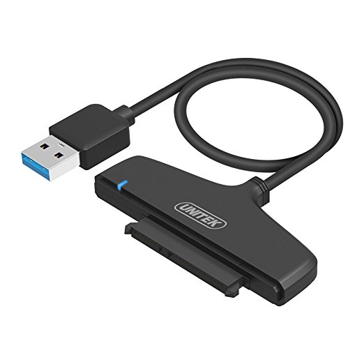
Supports 2.5″ SATA I/II/III hard drive/solid state drive. USB 3.0 supports data transfer speeds up to 5Gbps. Backwards compatible with USB2.0/USB1.0
Efficient UASP Transfer Protocol. An Equipped Cover provides better dust protecting SATA connector from dust.
Portable and lightweight design make it is easy to carry. LED light shows Power and Activity status.
Support hot swapping, easy and tool-free installation. No drivers or software needed
What We Offer – Unitek USB 3.0 to SATA 6G Adapter x1, 2-year warranty quality guarantee, 24h friendly customer service and email support

")