
Particle accelerators range in size from a room to a city. However, now scientists are looking closer at chip-sized electron accelerators, a new study finds. Potential near-term applications for the technology include radiation therapy for zapping skin cancer and, longer-term, new kinds of laser and light sources.
Particle accelerators generally propel particles within metal tubes or rings. The rate at which they can accelerate particles is limited by the peak fields the metallic surfaces can withstand. Conventional accelerators range in size from a few meters for medical applications to kilometers for fundamental research. The fields they use are often on the scale of millions of volts per meter.
In contrast, electrically insulating dielectric materials (stuff that doesn’t conduct electricity well but does support electrostatic fields well) can withstand light fields thousands of times stronger. This has led scientists to investigate creating dielectric accelerators that rely on lasers to hurl particles.
[…]
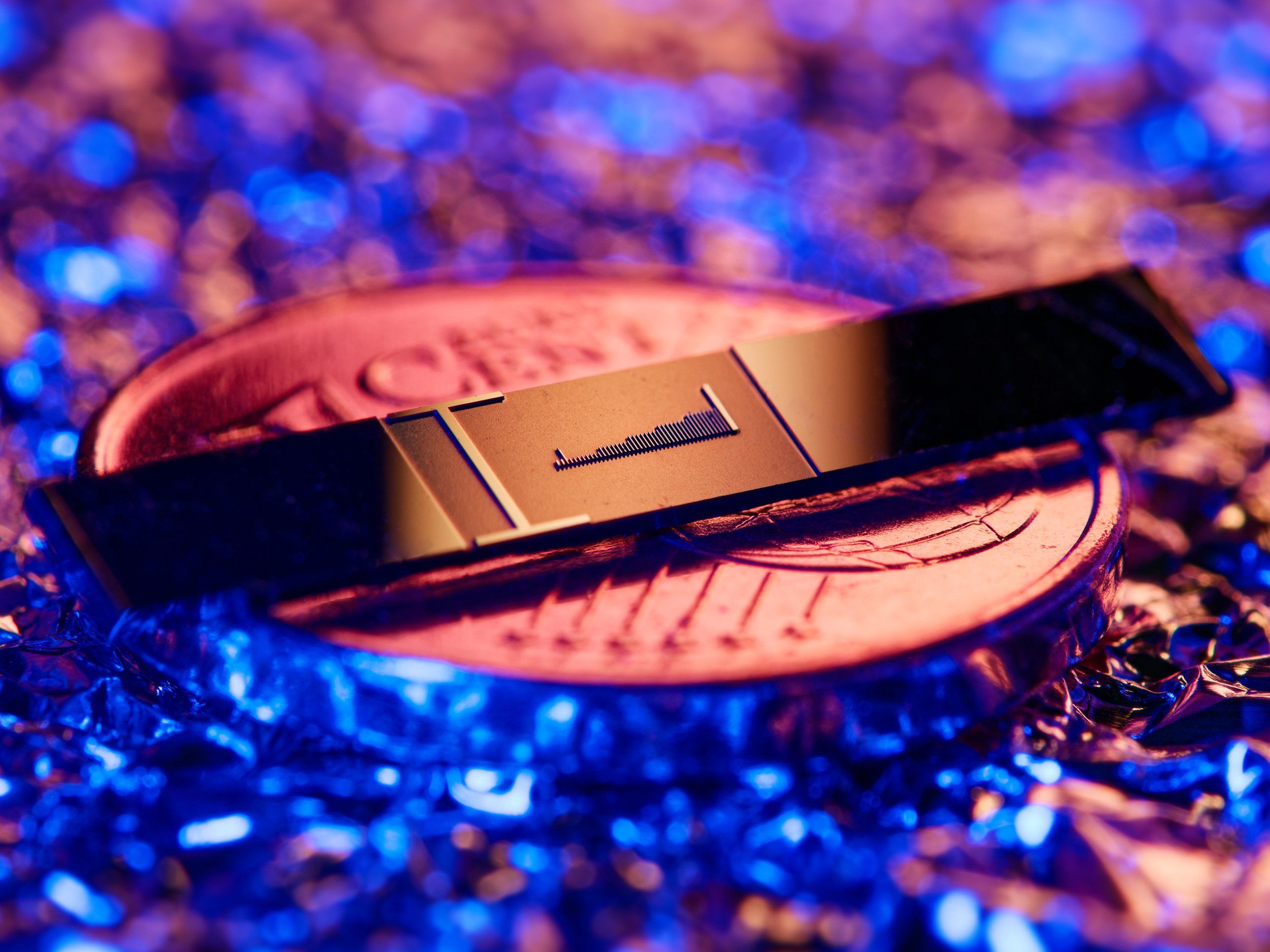
physicists fabricated a tiny channel 225 nanometers wide and up to 0.5 millimeters long. An electron beam entered one end of the channel and exited the other end.
The researchers shone infrared laser pulses 250 femtoseconds long on top of the channel to help accelerate electrons down it. Inside the channel, two rows of up to 733 silicon pillars, each 2 micrometers high, interacted with these laser pulses to generate accelerating forces.
The electrons entered the accelerators with an energy of 28,400 electron-volts, traveling at roughly one-third the speed of light. They exited it with an energy of 40,700 electron-volts, a 43 percent boost in energy.
This new type of particle accelerator can be built using standard cleanroom techniques, such as electron beam lithography. “This is why we think that our results represent a big step forward,” Hommelhoff says. “Everyone can go ahead and start engineering useful machines from this.”
[…]
Applications for these nanophotonic electron accelerators depend on the energies they can reach. Electrons of up to about 300,000 electron-volts are typical for electron microscopy, Hommelhoff says. For treatment of skin cancer, 10 million electron-volt electrons are needed. Whereas such medical applications currently require an accelerator 1 meter wide, as well as additional large, heavy and expensive parts to help drive the accelerator, “we could in principle get rid of both and have just a roughly 1-centimeter chip with a few extra centimeters for the electron source,” adds study lead author Tomáš Chlouba, a physicist at the University of Erlangen-Nuremberg in Germany.
Applications such as synchrotron light sources, free electron lasers, and searches for lightweight dark matter appear with billion electron-volt electrons. With trillion electron-volt electrons, high-energy colliders become possible, Hommelhoff says.
The scientists note there are many ways to improve their device beyond their initial proof-of-concept structures. They now aim to experiment with greater acceleration and higher electron currents to help enable applications, as well as boosting output by fabricating many accelerator channels next to each other that can all be driven by the same laser pulses.
In addition, although the new study experimented with structures made from silicon due to the relative ease of working with it, “silicon is not really a high-damage threshold material,” Hommelhoff says. Structures made of glass or other materials may allow much stronger laser pulses and thus more powerful acceleration, he says.
The researchers are interested in building a small-scale accelerator, “maybe with skin cancer treatment applications in mind first,” Hommelhoff says. “This is certainly something that we should soon transfer to a startup company.”
The scientists detailed their findings in the 19 October issue of the journal Nature.
Source: Particle Accelerator on a Chip Hits Penny-Size – IEEE Spectrum

Robin Edgar
Organisational Structures | Technology and Science | Military, IT and Lifestyle consultancy | Social, Broadcast & Cross Media | Flying aircraft